Method and device for attaching silicon nano particle film to surface of silicon solar cell

A silicon nanoparticle, silicon solar cell technology, applied in nanotechnology, nanotechnology, nanostructure manufacturing, etc., can solve the problems of reducing the cost of silicon solar cells, low yield of silicon nanoparticle, unsuitable for industrial production, etc. Low, efficient, easy to control effects

Active Publication Date: 2010-11-17
ZHEJIANG UNIV
View PDF2 Cites 0 Cited by
  • Summary
  • Abstract
  • Description
  • Claims
  • Application Information

AI Technical Summary

Problems solved by technology

Although they observed that the efficiency of silicon solar cells increased when the surface was covered with a thin film of silicon nanoparticles, their process was difficult to significantly reduce the cost of silicon solar cells
The main reasons are: (1) the yield of silicon nanoparticles obtained by electrochemical etching of silicon wafers is low and the cost is high; (2) the method of forming silicon nanoparticle films by dripping silicon nanoparticle solutions is not suitable for industrial production

Method used


Image

  • Method and device for attaching silicon nano particle film to surface of silicon solar cell
  • Method and device for attaching silicon nano particle film to surface of silicon solar cell

Examples


Embodiment 1

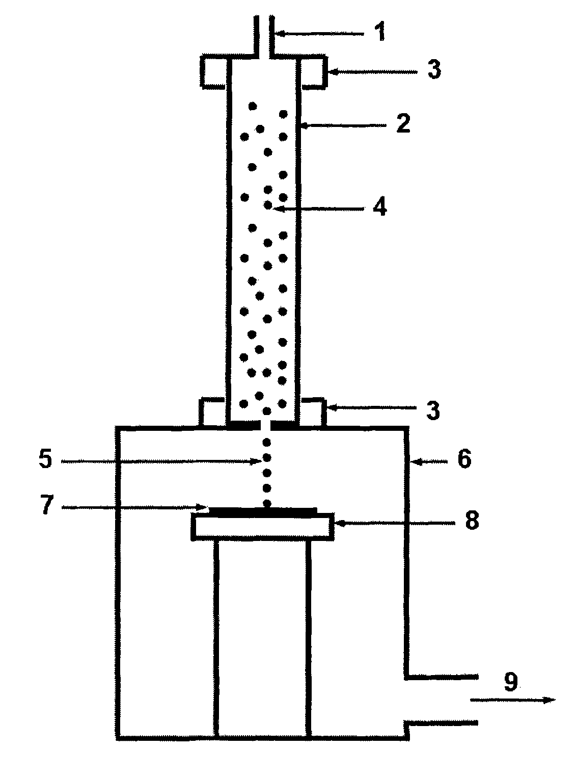
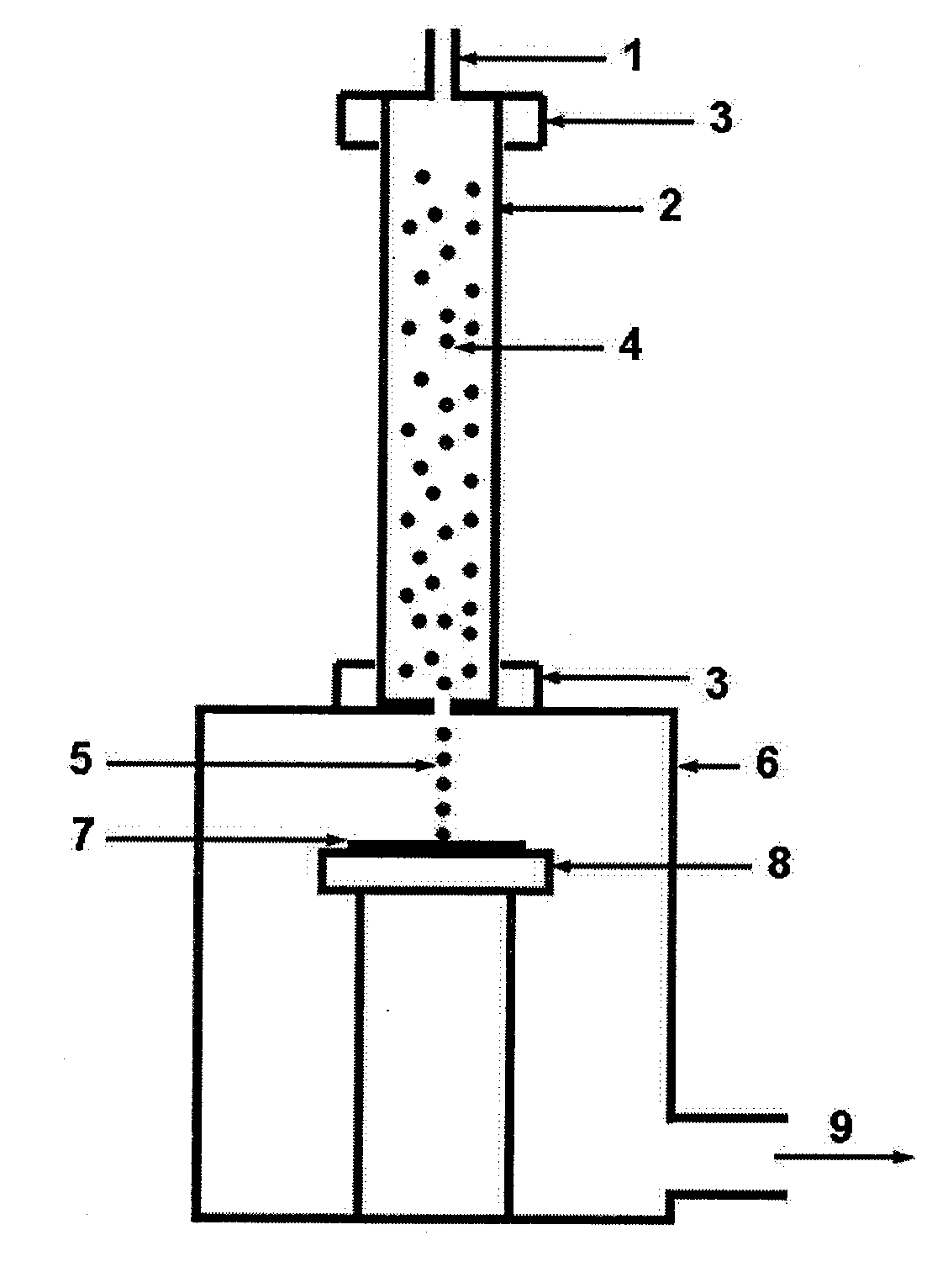
[0027] Such as figure 1 As shown, the device of the present invention for attaching a silicon nanoparticle film on the surface of a silicon solar cell includes a raw material chamber for preparing silicon nanoparticles and a film forming chamber 6 for placing a silicon solar cell. The raw material chamber is provided with an air inlet pipeline The tubular plasma chamber 2 (quartz tube) of 1, the intake pipeline 1 and the plasma chamber 2 are connected to each other through stainless steel connectors 3.

[0028] A high-frequency electromagnetic field emission device (not shown in the figure) is arranged on the periphery of the plasma chamber 2, so that the raw material gas entering the plasma chamber 2 is excited to generate silicon nanoparticles 4.

[0029] The plasma chamber 2 has an injection hole communicating with the film-forming chamber 6, the bottom of the film-forming chamber 6 is provided with a vacuum pipeline 9 for connecting to a vacuum system, and the film-forming...

Embodiment 2

[0034]Using the device of Embodiment 1, silane, argon and hydrogen are mixed and then enter the plasma chamber 2 through the inlet pipe 1 . The mixed gas forms a plasma under the excitation of a 13.56MHz radio frequency power supply, and silicon nanoparticles 4 are generated in the plasma, with an average size of 5.3nm and a standard deviation of size distribution of 0.7nm. The pressure in the plasma chamber 2 is 450Pa. Silicon nanoparticles 4 enter the stainless steel film-forming chamber 6 with a pressure of 4Pa in the form of silicon nanoparticle beams 5 after passing through the injection hole (round hole) with a diameter of 2 mm at the bottom of the plasma chamber 2 .

[0035] The silicon solar cell 7 whose surface is a grid-like metal electrode and an anti-reflection layer is placed on the sample stage 8 in the film forming chamber 6 . The vacuum of the whole system is achieved by vacuum pumping. The vacuum pump communicates with the film forming chamber 6 through a va...

Embodiment 3

[0038] Using the device of Embodiment 1, silane, argon and hydrogen are mixed and then enter the plasma chamber 2 through the inlet pipe 1 . The mixed gas forms a plasma under the excitation of a 13.56MHz radio frequency power supply, and silicon nanoparticles 4 are generated in the plasma, with an average size of 8.2nm and a standard deviation of size distribution of 1.1nm. The pressure in the plasma chamber 2 is 1060Pa. Silicon nanoparticles 4 enter the stainless steel film-forming chamber 6 with a pressure of 0.3Pa in the form of silicon nanoparticle beams 5 after passing through the injection hole (round hole) with a diameter of 1 mm at the bottom of the plasma chamber 2 .

[0039] The silicon solar cell 7 whose surface is a grid-like metal electrode and an anti-reflection layer is placed on the sample stage 8 in the film forming chamber 6 . The vacuum of the whole system is achieved by vacuum pumping. The vacuum pump communicates with the film forming chamber 6 through ...


PUM

PropertyMeasurementUnit
thicknessaaaaaaaaaa
sizeaaaaaaaaaa
sizeaaaaaaaaaa

Abstract

The invention discloses a method for attaching a silicon nano particle film to the surface of a silicon solar cell, which makes silicon nano particles form silicon nano particle beams, scans the silicon nano particle beams and attaches the silicon nano particle beams to the surface of the silicon solar cell to form the uniform silicon nano particle film. The invention also discloses a device for preparing the film, which comprises a raw material cavity and a film-forming cavity, wherein the raw material cavity is provided with a spray hole which is communicated with the film-forming cavity; the film-forming cavity is connected with a vacuum system; a sample platform which is used for bearing the silicon solar cell and can move tridimensionally is arranged inside the film-forming cavity; and after the silicon nano particles enter the film-forming cavity in the form of the silicon nano particle beams from the spray hole of the raw material cavity, the sample platform drives the silicon solar cell to move, and the silicon nano particle film is formed on the surface of the silicon solar cell. The method can effectively control the film-forming speed of the silicon nano particles on thesurface of the silicon solar cell and the thickness and the uniformity of the obtained silicon nano particle film, can improve the efficiency of the silicon solar cell, and is favorable for reducingthe cost of the silicon solar cell.

Description

technical field [0001] The invention relates to the field of photoelectric materials, in particular to a method and a device for attaching a silicon nanoparticle thin film on the surface of a silicon solar cell for improving the efficiency of the silicon solar cell. Background technique [0002] With the development of the global economy, the consumption of energy has increased dramatically. Currently, the vast majority of energy is obtained by burning fossil fuels. The huge amount of carbon dioxide and other gas emissions caused by the huge use of fossil fuels is causing increasingly serious social and environmental problems. Therefore, the development and utilization of various renewable energy sources has received more and more attention from the international community. Among all kinds of renewable energy, solar energy has become the focus of development because of its inexhaustible, inexhaustible, pollution-free, and convenient features. The utilization of solar ener...

Claims


Application Information

Patent Timeline
Patent Type & Authority Patents(China)
IPC IPC(8): H01L31/18B82B3/00
CPCY02P70/50
Inventor 皮孝东杨德仁
Owner ZHEJIANG UNIV
Why Eureka
Try Eureka