Resistance variable element, resistance variable storage device and resistance variable device
A technology of variable resistance and memory devices, which is applied in the field of variable resistance devices, variable resistance memory devices and variable resistance devices, and can solve the problems of miniaturization limit of FLASH memory, etc.
- Summary
- Abstract
- Description
- Claims
- Application Information
AI Technical Summary
Problems solved by technology
Method used
Image
Examples
no. 1 approach
[0101] [structure]
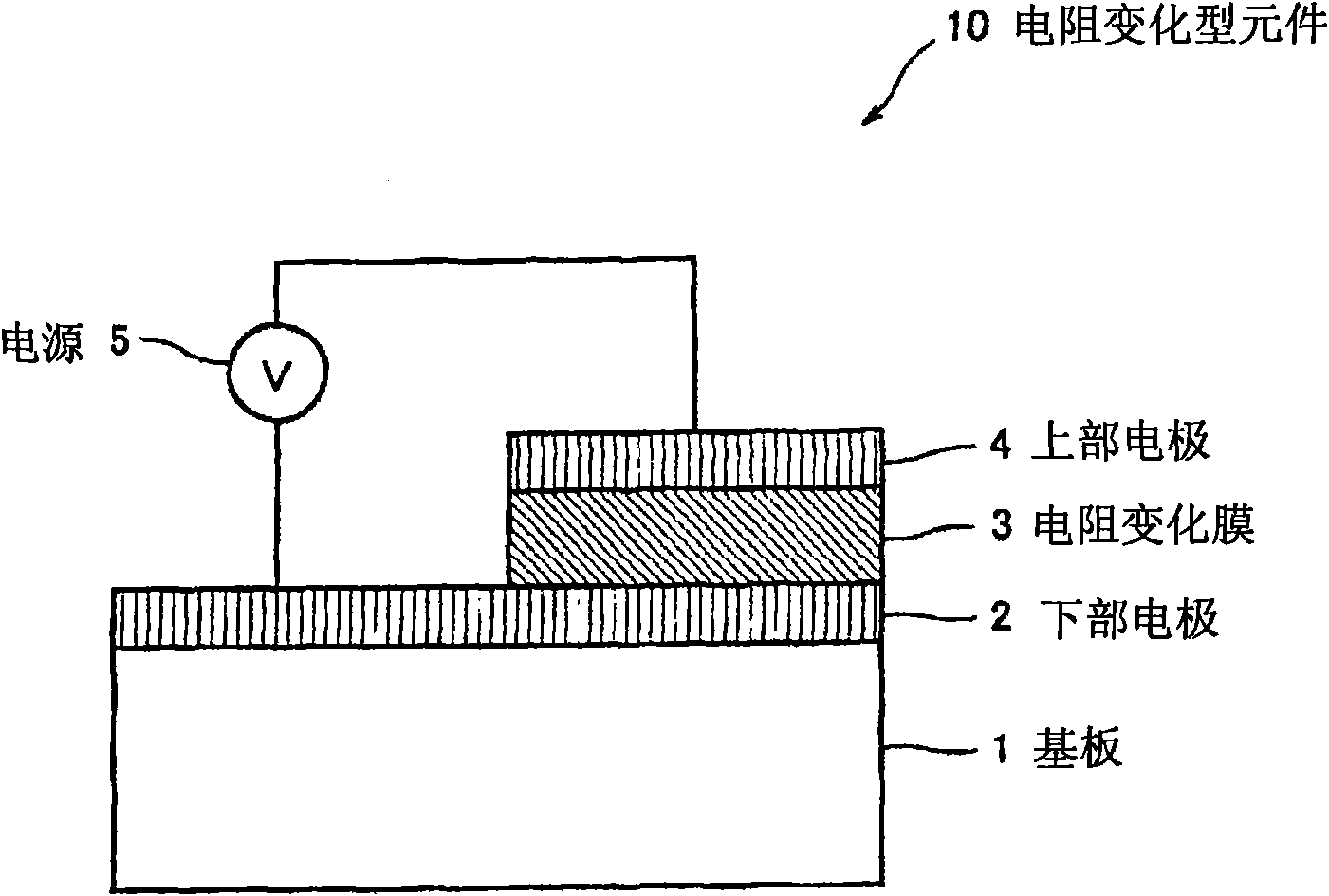
[0102] figure 1 It is a schematic diagram showing an example of the structure of the variable resistance element according to the first embodiment of the present invention.
[0103] Such as figure 1 As shown, the variable resistance element 10 of this embodiment includes a substrate 1, a lower electrode 2 (first electrode) formed on the substrate 1, a variable resistance layer 3 formed on the lower electrode 2, and a variable resistance layer 3 formed on the variable resistance layer 3. on the upper electrode 4 (second electrode). The lower electrode 2 and the upper electrode 4 are electrically connected to the variable resistance layer 3 , respectively. In addition, the upper electrode 4 may be a first electrode, and the lower electrode 2 may be a second electrode.
[0104] The substrate 1 is made of, for example, a silicon substrate.
[0105] The lower electrode 2 and the upper electrode 4 can be selected from, for example, Ag (silver), Au (gold), P...
Embodiment 1
[0142] On the silicon substrate, a lower electrode (20 μm×20 μm in size) made of Pt was formed by sputtering to a thickness of 0.2 μm. Prepare NiFe 2 o 4 and Fe 3 o 4 The targets are discharged simultaneously by sputtering, and a mask and lithography are used to form a layer with (Ni X Fe 1-X )Fe 2 o 4 The resistance change layer of the spinel structure represented by the chemical formula (size is 10 μm × 10 μm: area 100 μm 2 ). The substrate temperature when forming the variable resistance layer was 300°C. The size of the contact portion between the lower electrode and the variable resistance layer is 2 μm×2 μm (area 4 μm 2 ). The thickness of the variable resistance layer was 100 nm. Furthermore, on the variable resistance layer, an upper electrode (2 μm×2 μm in size) made of Pt was formed by sputtering using a mask and lithography to a thickness of 0.2 μm to obtain a variable resistance element. The size of the contact portion between the upper electrode and the...
Embodiment 2
[0150] In Example 2, the resistance variable element was formed in the same manner as in Example 1 except for the difference in parameters, and writing and reading were performed.
[0151] That is, in Example 2, the voltage applied to each target was adjusted so that the (Ni X Fe 1-X )Fe 2 o 4 The value of X is 0.65. The value of X was verified by combining two kinds of the RBS (Rutherford backscattering) method and the fluorescent X-ray analysis method. As a result of the verification, the value of X is 0.65. The resistivity was measured by the 4-terminal 4-probe method. The resistivity of the variable resistance layer of Example 2 was 10 Ωcm.
[0152]It was confirmed that the resistance variable element of this example has non-volatility in which the resistance value does not change even when the power supply is turned off. In addition, when the magnitude of the current flowing when the voltage pulse was applied was measured, it was 1 mA or less. Therefore, it can be...
PUM
 Abstract
Description
Claims
Application Information


