polarized light emitting diode

A light-emitting diode, polarization technology, applied in the direction of electrical components, circuits, semiconductor devices, etc., to achieve the effect of overall volume reduction, cost reduction, and performance optimization

Inactive Publication Date: 2011-12-21
SUZHOU UNIV
View PDF3 Cites 1 Cited by
  • Summary
  • Abstract
  • Description
  • Claims
  • Application Information

AI Technical Summary

Problems solved by technology

However, so far, the idea of ​​designing the structure of the LED chip itself in order to realize an efficient polarized light output LED has not been reported.

Method used


Image

  • polarized light emitting diode
  • polarized light emitting diode
  • polarized light emitting diode

Examples


Embodiment 1

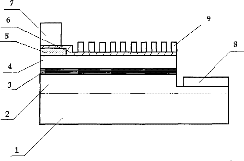
[0026] See attached figure 1 , which is a schematic cross-sectional view of the structure of a relief-type polarized light-emitting diode chip provided in this embodiment. The structure of the polarized light-emitting diode chip prepared on the surface of the III-V gallium nitride-based LED is as follows: an LED light-emitting working area is grown on the substrate material 1, including n-type GaN region 2, p-type GaN region 4 and InGaN / GaN Quantum well 3; on the p-type GaN region, there is an insulating dielectric film 5 in sequence, and the insulating medium is SiO 2 or SiN; p-type layer transparent electrode 6; p-type layer metal electrode 7 and relief metal film grating 9; and n-type layer metal electrode 8 on the n-type GaN region exposed by etching.

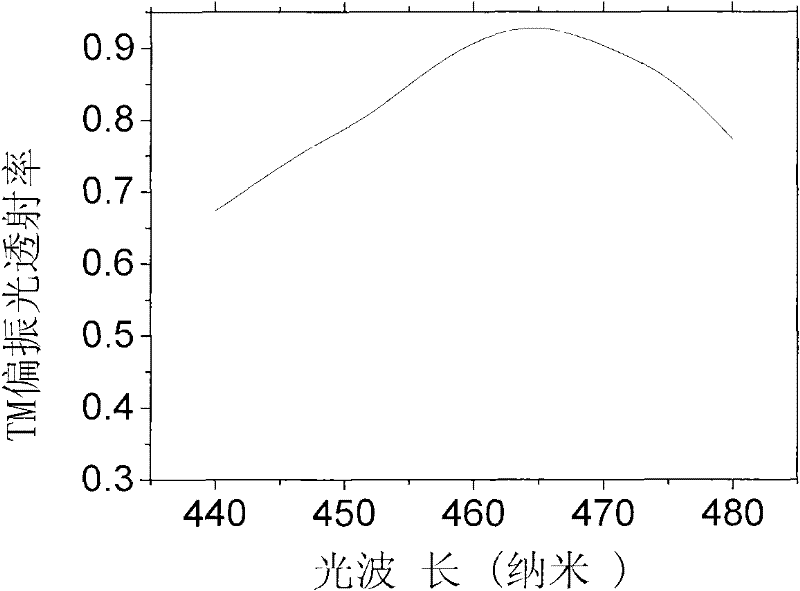
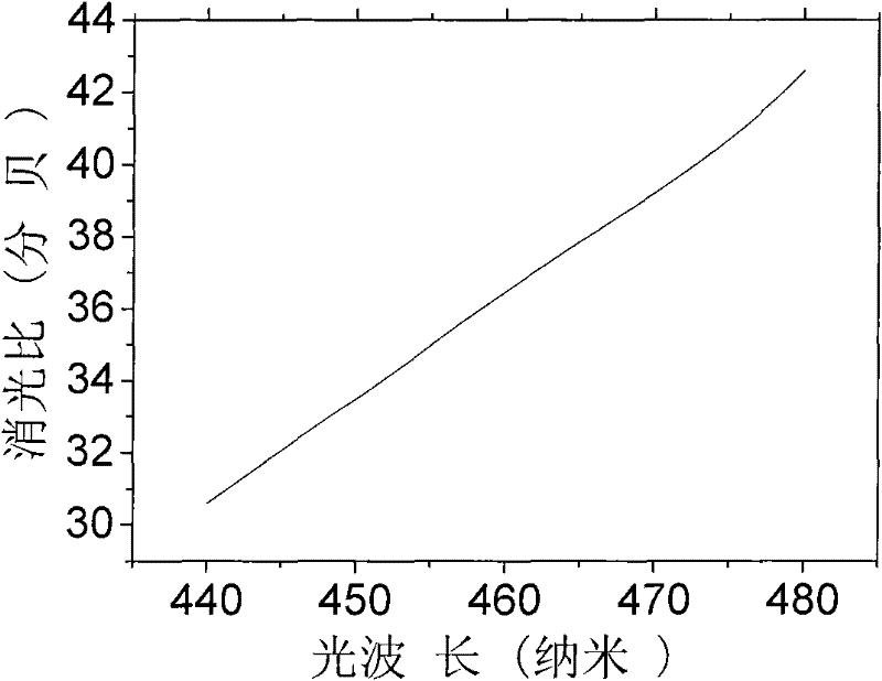
[0027] The shape, period, duty cycle, and thickness of the grating are theoretically calculated according to the specific luminous wavelength of the LED. The combination of the best polarization extinction ratio and trans...

Embodiment 2

[0037] See attached Figure 4 , which is a structural cross-sectional schematic diagram of an embedded polarized light-emitting diode chip provided in this embodiment; the embedded polarized light-emitting diode chip prepared on the surface of a III-V gallium nitride-based LED includes: substrate material 1; n-type GaN layer 2; InGaN / GaN quantum well 3; p-type GaN layer 4; SiO 2 Insulating dielectric film 5; p-type layer transparent electrode 6; p-type layer metal electrode 7; n-type layer metal electrode 8 and embedded metal GaN grating 10.

[0038] Compared with the structure of Example 1, the difference lies in that the periodic grating of this structure is prepared on the p-type layer of GaN, and the grating is formed by the concavo-convex structure of GaN.

[0039] In this embodiment, it is determined by calculation that the shape of the grating is a rectangle, the duty ratio of the grating is 0.52, the thickness of the grating is 300nm, and the period of the grating is ...


PUM


Abstract

The invention discloses a polarized light emitting diode. Its light-emitting diode chip includes a working area composed of an n-type region, a p-type region and a quantum well structure, a substrate, an insulating dielectric film, a transparent electrode and a metal electrode; it is characterized in that: a relief is prepared on the light-emitting surface of the light-emitting diode chip Type or embedded grating, the period of the grating is 50-600nm, the duty ratio is 0.2-0.9, and the thickness is 50-400nm. Compared with the traditional LED external polarizing plate to achieve polarization, the present invention adopts the technical scheme of directly integrating the grating structure on the surface of the LED chip, without the need for an external polarizing plate and other structures, and realizes the purpose of polarized light from the LED chip , therefore, the overall volume of the light-emitting device is greatly reduced, the performance is optimized, and the cost is reduced. At the same time, it can be integrated on the light-emitting chip at one time through the semiconductor photolithography process, which is easy to realize industrialization and popularization and application.

Description

technical field [0001] The invention relates to a light-emitting diode (LED), in particular to a light-emitting diode with polarized light output. Background technique [0002] A light emitting diode (LED) is a semiconductor light source device that is stimulated to emit light when electrically biased in the forward direction. The basic principle of LED light emission is: when the semiconductor chip with pn junction structure is applied, electrons and holes are injected from the n-type region and p-type region respectively, and the recombination of electrons and holes is expressed as photons. The form releases energy, and the emission wavelength depends on the forbidden band width of the material. At present, common LEDs include Al-In-Ga-N series of third-generation semiconductors that emit purple, blue, and green, Al-In-Ga-P series that emit yellow light, and Al-In-Ga-As that emit red light. series, and the ZnO series that is currently under rapid development. [0003] A...

Claims


Application Information

Patent Timeline
Patent Type & Authority Patents(China)
IPC IPC(8): H01L33/00
Inventor 曹冰张桂菊韩琴王钦华
Owner SUZHOU UNIV
Why Eureka
Try Eureka