GaAs based InAs/GaSb superlattice near infrared photodetector and manufacturing method thereof

A technology of electrical detectors and infrared light, applied in optical radiation measurement, radiation pyrometry, instruments, etc., can solve the problems of no semi-insulating substrate, difficult to read out circuit integration, and expensive GaSb substrate, etc., to achieve The detection rate, low cost, and the effect of improving the detection rate

Inactive Publication Date: 2009-11-11
INST OF SEMICONDUCTORS - CHINESE ACAD OF SCI
View PDF0 Cites 11 Cited by
  • Summary
  • Abstract
  • Description
  • Claims
  • Application Information

AI Technical Summary

Problems solved by technology

[0004] Although InAs/GaSb superlattice growth can obtain less defect density on the matched GaSb substrate, the GaSb substrate has a series of disadvantages such as expensive, no semi-insulating substrate, and difficult

Method used


Image

  • GaAs based InAs/GaSb superlattice near infrared photodetector and manufacturing method thereof
  • GaAs based InAs/GaSb superlattice near infrared photodetector and manufacturing method thereof
  • GaAs based InAs/GaSb superlattice near infrared photodetector and manufacturing method thereof

Examples


Embodiment Construction

[0034] In order to make the object, technical solution and advantages of the present invention clearer, the present invention will be described in further detail below in conjunction with specific embodiments and with reference to the accompanying drawings.

[0035] Taking an InAs / GaSb infrared detector with a cut-off detection wavelength near 2.5 μm at room temperature as an example, the specific implementation of the present invention will be further described in detail in conjunction with the accompanying drawings:

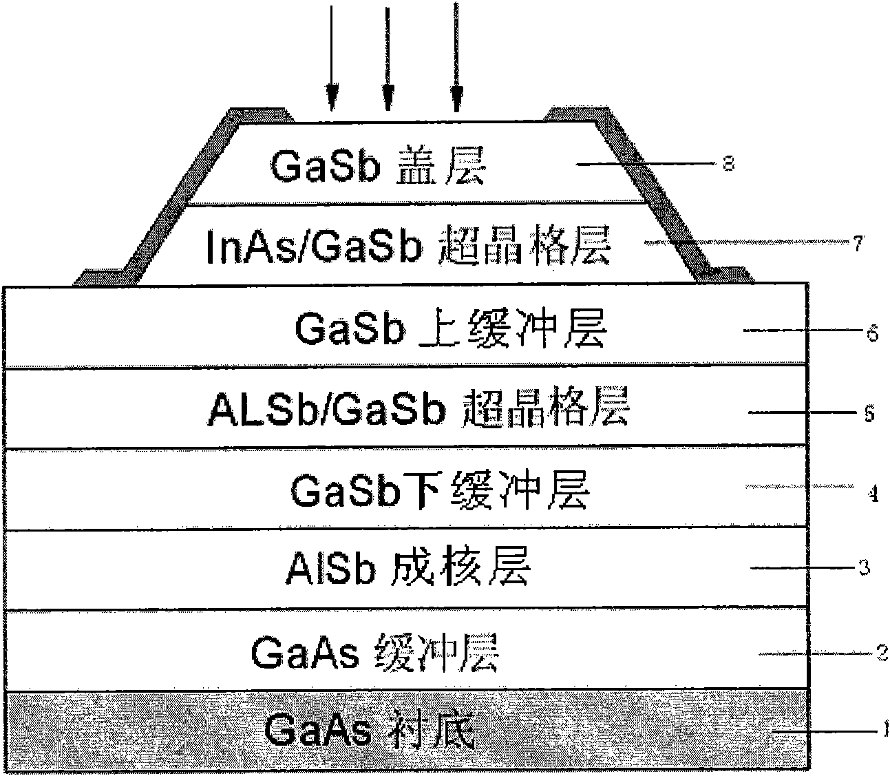
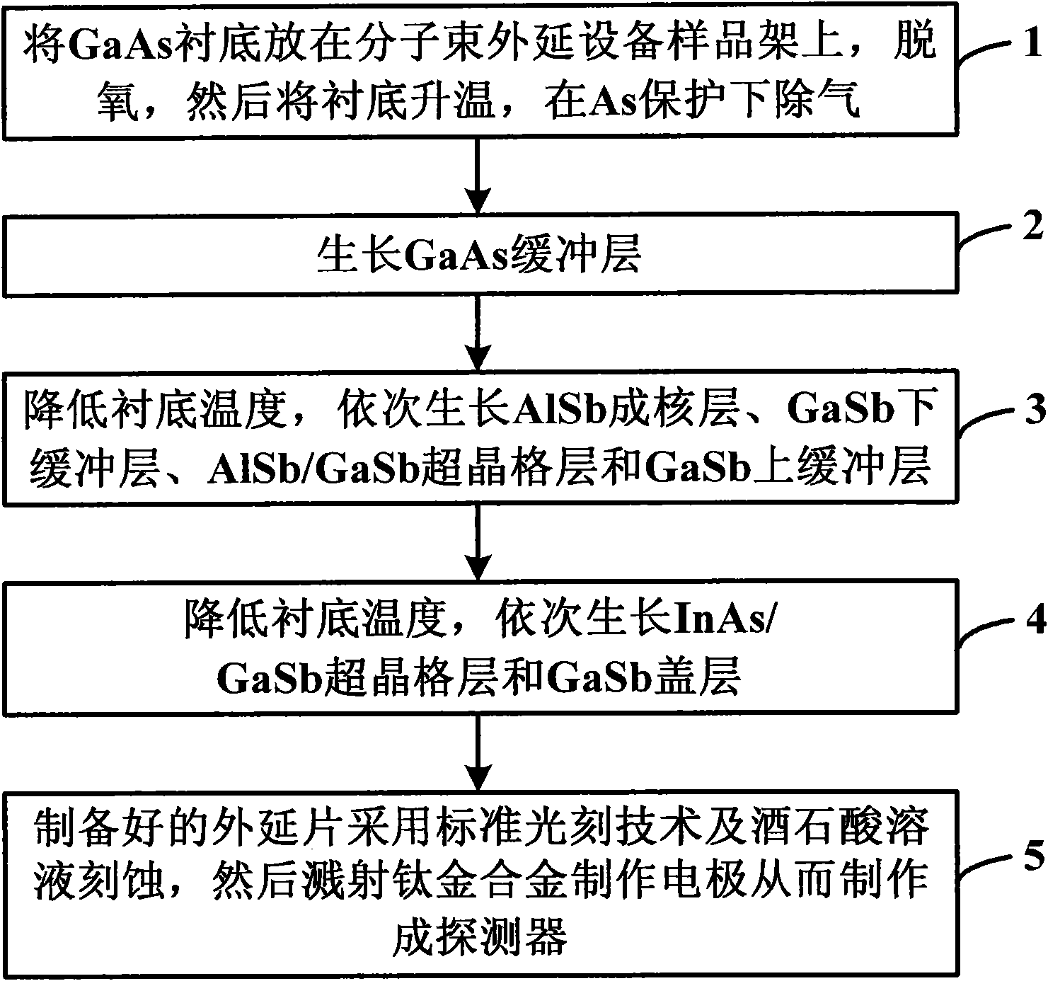
[0036] Such as figure 1 as shown, figure 1 It is a structural schematic diagram of the InAs / GaSb superlattice infrared photodetector provided by the present invention. The infrared photodetector consists of a bottom-up GaAs substrate, a GaAs buffer layer, an AlSb nucleation layer, a GaSb lower buffer layer, an AlSb / It consists of a GaSb superlattice layer, a GaSb upper buffer layer, an InAs / GaSb superlattice layer, a GaSb capping layer and a titanium-gold all...


PUM

PropertyMeasurementUnit
Thicknessaaaaaaaaaa
Thicknessaaaaaaaaaa
Thicknessaaaaaaaaaa

Abstract

The invention discloses a GaAs based InAs/GaSb superlattice 1-3 micron band near infrared photodetector, which consists of the following components from bottom to top: a GaAs substrate, a GaAs buffer layer, an AlSb nucleating layer, a GaSb lower buffer layer, an AlSb/GaSb superlattice layer, a GaSb upper buffer layer, an InAs/GaSb superlattice layer, a GaSb cover layer and a titanium alloy electrode. The invention also discloses a method for manufacturing the GaAs based InAs/GaSb superlattice 1-3 micron band near infrared photodetector at the same time. By using the GaAs based InAs/GaSb superlattice 1-3 micron band near infrared photodetector and the method, a high-quality GaSb buffer layer is grown on the GaAs substrate, and the InAs/GaSb superlattice layer is grown on the GaSb buffer layer, thus an infrared photodetector with low dark current and low cost can be manufactured.

Description

technical field [0001] The invention relates to the field of infrared photodetectors in semiconductor technology, in particular to a GaAs-based InAs / GaSb superlattice infrared photodetector with a wavelength of 1 to 3 microns and a manufacturing method thereof. Background technique [0002] With the advancement of science and technology, infrared detectors with military use as the core have gradually developed. Atmospheric monitoring and other military and civilian fields have a wide range of applications. [0003] However, the most commonly used silicon-doped detectors, InSb, QWIP, MCT and other infrared detectors are all required to work at low temperature, require special refrigeration equipment, and are expensive, so their applications are limited. The InAs / GaSb infrared detector is due to the particularity of its materials, for example: the high effective mass of electrons and holes can effectively reduce the tunneling current and increase the density of states; the en...

Claims


Application Information

Patent Timeline
IPC IPC(8): G01J5/00
Inventor 汤宝周志强郝瑞亭任正伟徐应强牛智川
Owner INST OF SEMICONDUCTORS - CHINESE ACAD OF SCI
Why Eureka
Try Eureka