Seed crystal support for growing silicon carbide crystal with high quality

A silicon carbide and seed crystal technology, applied in the direction of single crystal growth, crystal growth, single crystal growth, etc., can solve the problems of reducing the quality and yield of the wafer, and achieve the suppression of backside evaporation, elimination of planar hexagonal defects, and improvement of crystal quality and The effect of yield

Active Publication Date: 2009-11-18
BEIJING TIANKE HEDA SEMICON CO LTD
View PDF0 Cites 43 Cited by
  • Summary
  • Abstract
  • Description
  • Claims
  • Application Information

AI Technical Summary

Problems solved by technology

This defect is a killer defect, its formati...

Method used


Image

  • Seed crystal support for growing silicon carbide crystal with high quality
  • Seed crystal support for growing silicon carbide crystal with high quality
  • Seed crystal support for growing silicon carbide crystal with high quality

Examples


Embodiment Construction

[0023] The seed crystal support structure of the present invention will be described in detail below with reference to the accompanying drawings.

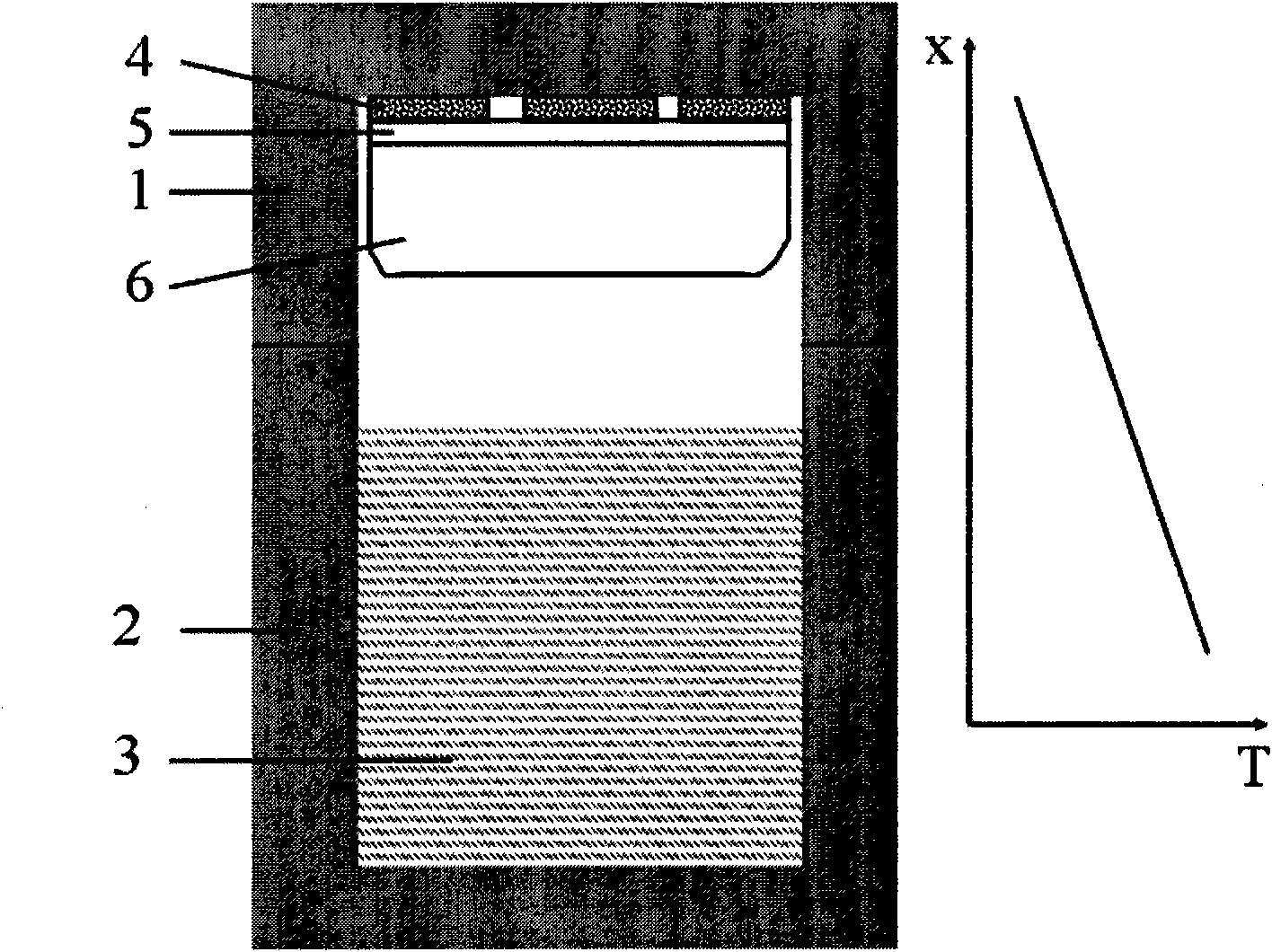
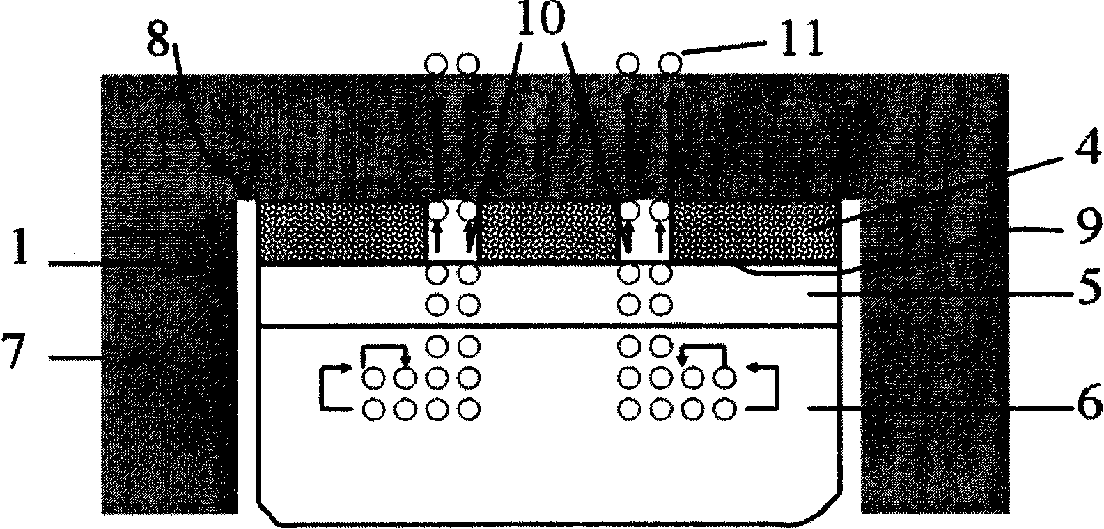
[0024] figure 2 It is a schematic diagram of the seed crystal support structure commonly used to grow SiC crystals at present. The graphite cover 1 is processed from Sangao graphite, and the flatness of its inner surface 8 is better than 10 μm. The seed crystal 5 is adhered to the inner surface 8 of the graphite cap 1 by means of an adhesive 4 . Due to factors such as poor machining accuracy and uneven bonding of the adhesive 4 , some pores 10 inevitably exist between the back surface 9 of the seed crystal and the inner surface 8 of the graphite cap 1 . The difference in thermal conductivity between the pores 10 and the binder 4 after high-temperature carbonization will lead to uneven temperature distribution on the rear surface 9 of the seed crystal. When the crystal grows, there is a certain temperature gradient in the growin...


PUM


Abstract

The invention provides a seed crystal support for growing a silicon carbide crystal with high quality by a physical vapor phase transport method. The seed crystal support comprises a graphite substrate and a compact film layer arranged on the surface of the graphite substrate. The compact film layer is stable and compact at high temperature and eliminates the defects of the graphite substrate caused by porosity. The compactness of the film layer inhibits steam generated by the back evaporation of the crystal from escaping from a hole of the graphite substrate, eliminates the planar hexagonal defect caused by back evaporation in the process of crystal growth and greatly improves the quality and the yield of the silicon carbide crystal.

Description

technical field [0001] The invention belongs to the field of crystal growth, in particular to a seed crystal support for growing high-quality silicon carbide crystals. Background technique [0002] Wide bandgap semiconductor materials represented by silicon carbide (SiC) and gallium nitride (GaN) are the third-generation semiconductors after silicon (Si) and gallium arsenide (GaAs). Compared with Si and GaAs traditional semiconductor materials, SiC has excellent properties such as high thermal conductivity, high breakdown field strength, high saturation electron drift rate and high bonding energy, and has great potential in high temperature, high frequency, high power and radiation resistant devices. Application prospects. In addition, due to the similar lattice constant and thermal expansion coefficient of SiC and GaN, it also has extremely broad application prospects in the field of optoelectronic devices. [0003] At present, the most effective method for growing SiC cr...

Claims


Application Information

Patent Timeline
IPC IPC(8): C30B23/00C30B29/36
Inventor 陈小龙彭同华杨慧王文军倪代秦王皖燕
Owner BEIJING TIANKE HEDA SEMICON CO LTD
Why Eureka
Try Eureka