Seed crystal treatment method and silicon carbide mono-crystal growing method

A silicon carbide single crystal and processing method technology, applied in the direction of single crystal growth, crystal growth, single crystal growth, etc., can solve the problems of reducing wafer quality and yield

Active Publication Date: 2011-03-16
XINJIANG TANKEBLUE SEMICON +1
View PDF1 Cites 44 Cited by
  • Summary
  • Abstract
  • Description
  • Claims
  • Application Information

AI Technical Summary

Problems solved by technology

This defect is a killer defect, its formati...

Method used


Image

  • Seed crystal treatment method and silicon carbide mono-crystal growing method
  • Seed crystal treatment method and silicon carbide mono-crystal growing method
  • Seed crystal treatment method and silicon carbide mono-crystal growing method

Examples


Embodiment 1

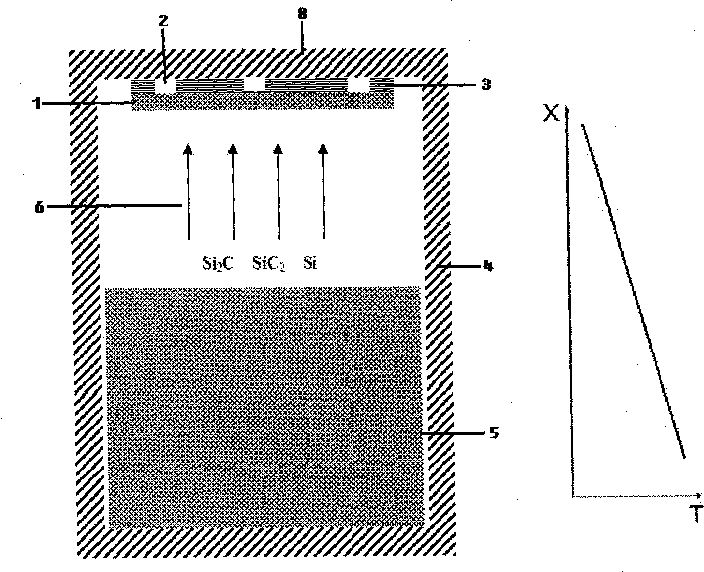
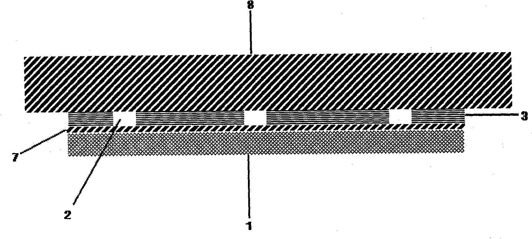
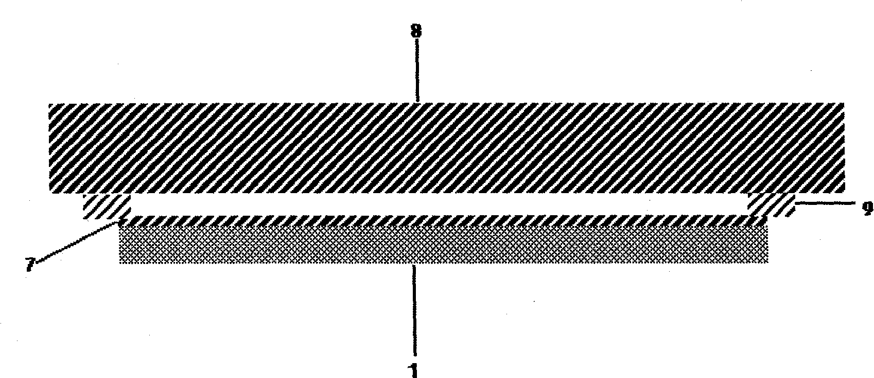
[0020] Take 0.5ml of the organic mixture (the mass percentage of furan methanol and phenolic resin is 3:1), apply it evenly on the back of the seed crystal with a coater, the thickness of the coating is 1 μm, and place it at room temperature for 24 hours to cure. The wafer is then gently placed in the graphite crucible with the organic coating side up. Put the graphite crucible into the graphite furnace again, pump the gas to 10 -3After Pa, the temperature was raised to 1000°C at a rate of 500°C / h, and the temperature was kept constant for 2 hours. Then fill it with argon gas 0.6 atm, raise the temperature at 500°C / h to 1800°C, keep the temperature for 1 hour, and finally cool it down to room temperature at the rate of 1000°C / h. After 8 hours, the graphite furnace was opened, and the wafer was taken out. There was a uniform graphite coating on the back of the wafer with a thickness of 1 μm.

Embodiment 2

[0022] Take 5ml of the organic mixture (the mass percentage of furan methanol and phenolic resin is 1:1), apply it evenly on the back of the seed crystal with a coater, the thickness of the coating is 30 μm, and place it at 60°C for 2 hours to cure. The wafer is then gently placed in the graphite crucible with the organic coating side up. Put the graphite crucible into the graphite furnace again, pump the gas to 10 -3 After Pa, it was raised to 1200°C at a rate of 500°C / h, and the temperature was kept constant for 1 hour. Then fill it with argon gas 0.6 atm, raise the temperature to 2200°C at 500°C / h, keep the temperature for 0.5 hours, and finally cool down to room temperature at the rate of 1000°C / h. After 8 hours, the graphite furnace was opened, and the wafer was taken out. There was a uniform graphite coating on the back of the wafer, with a thickness of 30 μm.

Embodiment 3

[0024] Take 10ml of the organic mixture (the mass percentage of furan methanol and phenolic resin is 1:3), apply it evenly on the back of the seed crystal with a coater, the coating thickness is 100μm, and place it at 80°C for 1 hour to cure. The wafer is then gently placed in the graphite crucible with the organic coating side up. Put the graphite crucible into the graphite furnace again, pump the gas to 10 -3 After Pa, it was raised to 1500°C at a rate of 500°C / h, and the temperature was kept constant for 0.5 hours. Then fill it with argon gas 0.6 atm, and raise the temperature to 2300°C at 500°C / h, keep the temperature for 0.5 hours, and finally cool down to room temperature at the rate of 1000°C / h. After 8 hours, the graphite furnace was opened, and the wafer was taken out. There was a uniform graphite coating on the back of the wafer with a thickness of 100 μm.

[0025] It should be noted that although the organic mixture of furan methanol and phenolic resin is used as ...


PUM


Abstract

The invention discloses a seed crystal treatment method for silicon carbide crystal growth and a silicon carbide mono-crystal growing method using the same. The seed crystal treatment method comprises the following steps: coating an organic substance on the back side, which is opposite to the growing side of the seed crystal, of the seed crystal, wherein the mass percentage of the carbon element in the organic substance is more than 50 percent; heating the seed crystal coated with the organic substance until the temperature thereof is between 1,000 and 2,300 DEG C to form a graphite film on the back side of the seed crystal; and cooling the seed crystal with the formed graphite film to obtain the seed crystal for preparing the silicon carbide crystal. The graphite coating treated by the method can maintain compactness and stability under the SiC mono-crystal growing condition so as to avoid back corrosion to a certain extent, and improve the quality and yield of the crystal.

Description

technical field [0001] The invention belongs to the field of crystal growth, and in particular relates to an improved process for growing high-quality silicon carbide crystals. Background technique [0002] With the maturity of the development of the first-generation silicon semiconductor and the second-generation gallium arsenide semiconductor materials, their device applications are also reaching their limits. More and more fields of modern science and technology require materials with high operating frequency, high power density, high temperature resistance, good chemical stability, and work in strong radiation environments. Therefore, the third-generation semiconductors (ie, wide-bandgap semiconductors, greater than 2.2eV) has received great attention, these materials include SiC, AlN, GaN, ZnO, diamond, etc., among which SiC is the most mature technology. SiC is an indirect bandgap semiconductor with wide bandgap, high thermal conductivity (higher than copper), high br...

Claims


Application Information

Patent Timeline
IPC IPC(8): C30B23/00C30B29/36
Inventor 王波陈小龙彭同华鲍慧强刘春俊李龙远王刚
Owner XINJIANG TANKEBLUE SEMICON
Why Eureka
Try Eureka