

A seed treatment method for growing high-quality silicon carbide crystals
A processing method and technology for silicon carbide seeds, which are applied in the field of seed crystal processing for growing high-quality silicon carbide crystals, can solve problems such as reducing the quality and yield of wafers, prevent backside evaporation, improve crystal quality and yield, and eliminate flat surfaces. Effects of Hexagonal Defects
- Summary
- Abstract
- Description
- Claims
- Application Information
AI Technical Summary
Problems solved by technology
Method used
Image

Examples
Embodiment 1
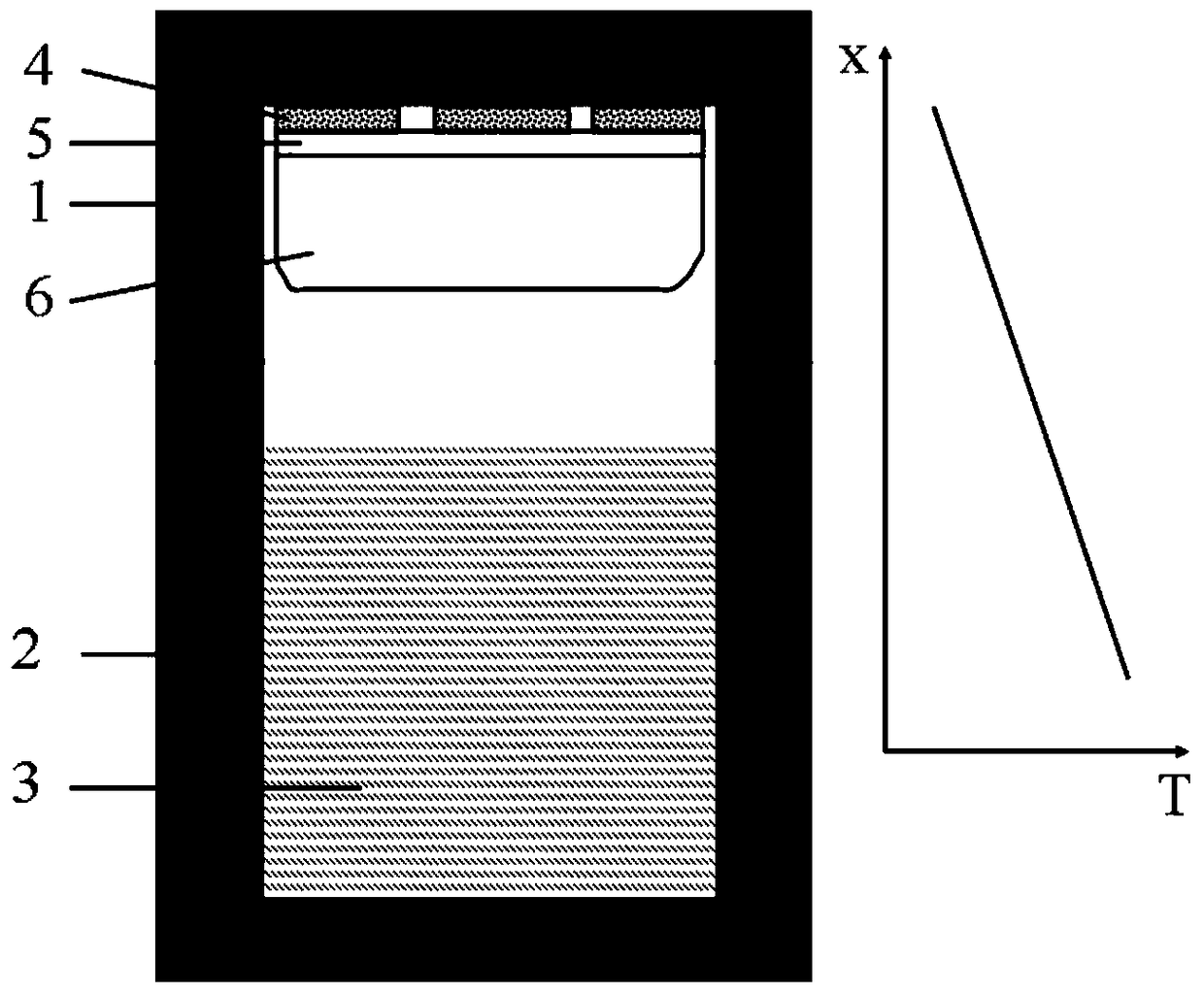
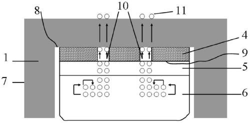
[0026] A piece of 4H-SiC seed crystal with a diameter of 100mm, the C surface is selected as the crystal growth surface, and the Si surface is the back side of the growth surface, that is, the coating coverage surface. Deposit a 0.2um thick yttrium oxide coating on the Si surface of 4H-SiC by magnetron sputtering, and then place the coated seed crystal and carbon powder in a protective atmosphere of Ar gas at 1 atmosphere and heat it to 2100°C Hold for 30 minutes to allow the carbon powder and yttrium oxide to react. After the reaction, the coating is a mixed coating of yttrium silicon carbide and yttrium carbide. Fix the seed crystal with the coating on the graphite support with an adhesive; then install the graphite support and the crucible together, place it in a silicon carbide single crystal furnace, and carry out the growth of silicon carbide crystals, and finally obtain 4H-SiC crystals one. Compared with the conventional seed crystal processing method, there is no obv...
Embodiment 2
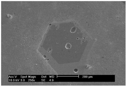
[0028]A piece of 6H-SiC seed crystal with a diameter of 76.2mm, the Si surface is selected as the crystal growth surface, and the C surface is the back surface, that is, the coating coverage surface. A yttrium silicon carbon coating with a thickness of 0.5um was deposited on the Si surface of 6H-SiC by chemical vapor deposition. Fix the seed crystal with the coating on the graphite support with an adhesive; then install the graphite support and the crucible together, place them in a silicon carbide single crystal furnace, and grow silicon carbide crystals to finally obtain 6H-SiC crystals one. Compared with the conventional seed crystal structure, there is no obvious sign of evaporation on the back of the crystal grown by this seed crystal treatment method. When the crystal is cut into a wafer, it is found that there is no planar hexagonal cavity defect inside the wafer, and the quality and yield of the silicon carbide wafer have been significantly improved.
Embodiment 3
[0030] A piece of 4H-SiC seed crystal with a diameter of 150 mm, the C surface is selected as the crystal growth surface, and the Si surface is the back side of the growth surface, that is, the coating coverage surface. A yttrium carbide coating with a thickness of 0.4um was deposited on the Si surface of 4H-SiC by magnetron sputtering. Subsequent silicon carbide crystal growth is performed on the seed crystal obtained by the seed crystal treatment method to obtain one 4H-SiC crystal. Compared with the conventional seed crystal structure, there is no obvious sign of evaporation on the back of the crystal grown by the seed crystal structure. When the crystal is cut into a wafer, it is found that there is no planar hexagonal cavity defect inside the wafer, and the quality and yield of silicon carbide wafers have been significantly improved.
PUM
| Property | Measurement | Unit |
|---|---|---|
| thickness | aaaaa | aaaaa |
| porosity | aaaaa | aaaaa |
Abstract
Description
Claims
Application Information