Cover layer of semiconductor device interconnected structure and manufacturing method thereof

A technology of interconnection structure and manufacturing method, which is applied in the direction of semiconductor devices, semiconductor/solid-state device manufacturing, semiconductor/solid-state device components, etc., and can solve the problems of easy chip breakage, chip burnout, and loss of electrical connection of metal wires in interconnection structures, etc. problem, achieve the effect of ensuring work efficiency and stability, reducing RC delay, and reducing parasitic capacitance

Inactive Publication Date: 2009-11-25
SEMICONDUCTOR MANUFACTURING INTERNATIONAL (BEIJING) CORP
View PDF1 Cites 11 Cited by
  • Summary
  • Abstract
  • Description
  • Claims
  • Application Information

AI Technical Summary

Problems solved by technology

[0006] In the existing method for making the interconnection structure of semiconductor devices, a single dielectric layer is generally used to form on the substrate of the interconnection structure of semiconductor devices, to seal the porous interlayer dielectric in the interlayer dielectric, or to seal the porous interlayer dielectric in the interlayer dielectric. The air gap is opened to form an air gap in the interlayer dielectric, which can reduce the parasitic capacitance between the metal wires of the semiconductor device interconnection structure to reduce the RC delay of signal transmission, but at the same time due to the porous structure or air in the interlayer dielectric The gap will also reduce the mechanical strength of the entire interconnection structure, making the chip easy to break during use, the electrical connection between the metal wires of the interconnection structure will be lost, and the circuit will not work normally; and the porous structure in the interlayer medium or The air gap usually also reduces the thermal conductivity of the entire interconnection structure, so that the heat generated by the circuit in the chip cannot be dissipated quickly, which may cause the inside of the chip to burn out due to excessive temperature, and then affect the entire circuit. Chip efficiency and stability

Method used


Image

  • Cover layer of semiconductor device interconnected structure and manufacturing method thereof
  • Cover layer of semiconductor device interconnected structure and manufacturing method thereof
  • Cover layer of semiconductor device interconnected structure and manufacturing method thereof

Examples


Embodiment Construction

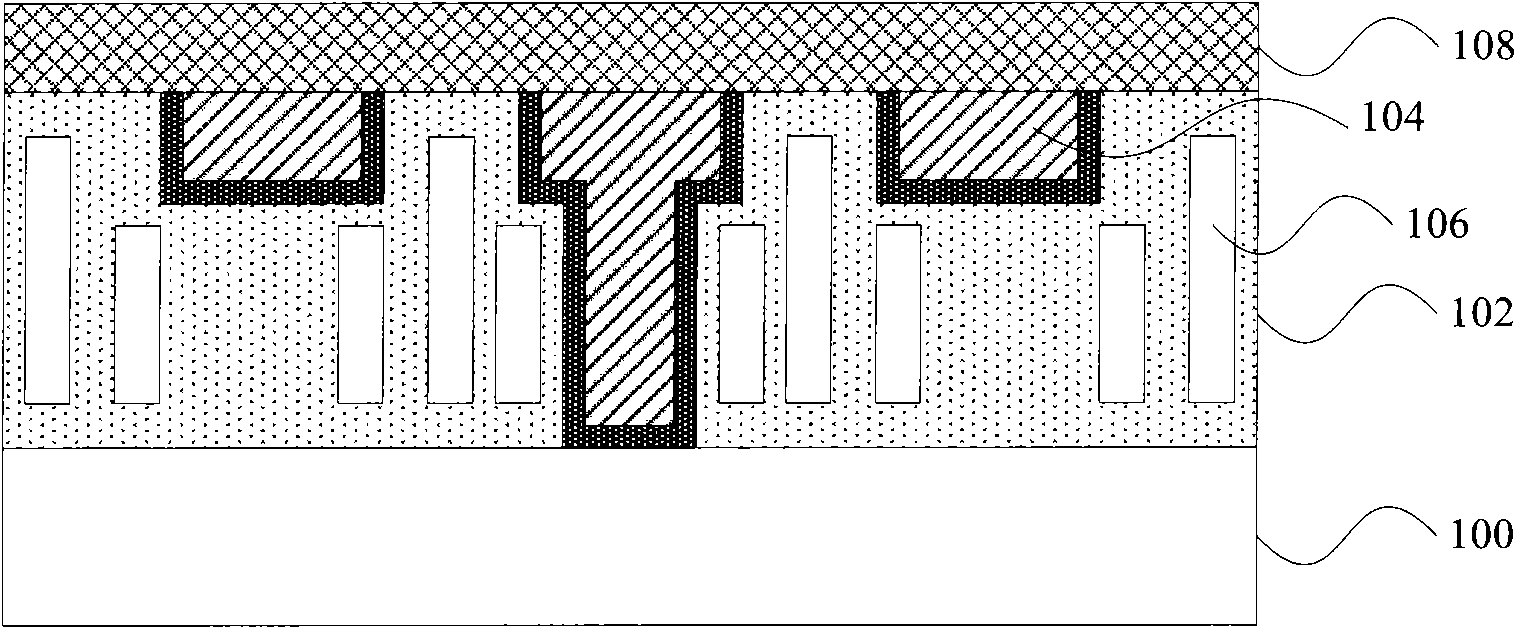
[0033] In the process of manufacturing the interconnection structure of semiconductor devices, the composite dielectric layer is used as a cover layer to protect the interlayer dielectric of each metal interconnection layer, so that the entire interconnection structure has higher mechanical strength and ensures that the chip is in use. Not easy to break. The composite dielectric layer enables the entire interconnection structure to use porous low-permittivity materials as the interlayer dielectric, and can also form air gaps in the interlayer dielectric without adversely affecting the mechanical strength of the interconnection structure, which can reduce the metal The parasitic capacitance between interconnect lines ultimately reduces the RC delay of IC signal transmission.

[0034] In addition, the metal material with high mechanical strength is used as the sandwich layer in the composite dielectric layer, which can further increase the mechanical strength of the interconnect...


PUM


Abstract

The invention relates to a manufacturing method for a cover layer of a semiconductor device interconnected structure. The manufacturing method comprises the following steps: providing a semiconductor device interconnected structure matrix provided with interlevel dielectrics; forming a bottom cover layer on the interlevel dielectrics; forming a first sandwich layer in the bottom cover layer; and forming a top cover layer on the bottom cover layer and the first sandwich layer. Correspondingly, the invention also provides the cover layer of the semiconductor device interconnected structure. The invention adopts a compound medium layer as the cover layer of the semiconductor device interconnected structure, improves the mechanical strength of the whole interconnected structure and ensures that a chip is not easy to break in the use process. While further improving the mechanical strength of the whole interconnected structure, the metal material with higher thermal conduction in the cover layer can easily and timely dissipate heat generated in the working process of the chip so as to ensure that the chip cannot be burned down due to overhigh temperature and ensure the working efficiency and the stability of the chip.

Description

technical field [0001] The invention relates to the technical field of semiconductor manufacturing, in particular to a cover layer of a semiconductor device interconnection structure and a manufacturing method thereof. Background technique [0002] One of the challenges encountered in the field of integrated circuit design and manufacturing today is how to reduce the RC delay (Resistive Capacitive delay) of signal transmission. In this regard, one of the methods that the current technology has adopted is to replace aluminum interconnects with copper interconnects. Reduce the series resistance of metal interconnection lines; Another method is to reduce the parasitic capacitance between metal interconnection lines, which can be achieved by constructing porous (Porous) low dielectric constant (Low dielectric constant) in the dielectric layer between metal interconnection lines. k) material or air gap (Air Gap) to achieve. [0003] In addition, when the integrated circuit is wo...

Claims


Application Information

Patent Timeline
Patent Type & Authority Applications(China)
IPC IPC(8): H01L21/768H01L23/522H01L23/532H01L23/373
CPCH01L2924/0002
Inventor 郭景宗肖德元
Owner SEMICONDUCTOR MANUFACTURING INTERNATIONAL (BEIJING) CORP
Why Eureka
Try Eureka