Dielectric layer structure for reducing stress and manufacturing method thereof

A manufacturing method and dielectric layer technology, which can be used in semiconductor/solid-state device manufacturing, circuits, electrical components, etc., and can solve problems such as grain bending

Inactive Publication Date: 2009-11-25
FUPO ELECTRONICS CORP
View PDF0 Cites 9 Cited by
  • Summary
  • Abstract
  • Description
  • Claims
  • Application Information

AI Technical Summary

Problems solved by technology

[0007] Wherein, after exposure and development processes are formed, the first dielectric layer 15 is formed with a second window 151 corresponding to expose the pad, as shown in Figure 3A , E, so the first dielectric layer 15 except for the setting of the second window 151, other areas are continuous area ranges, and the first dielectric layer 15 is polyimide (polyimide), benzocyclobutane (BCB; Benzocyclo-buthene), or silicone (silicone) and other high molecular polymer materials, when undergoing a heating and aging process, the first dielectric layer 15 will generate shrinkage stress due to temperature effects, making the overall wafer thinner and more flexible. Die bending occurs after cutting

Method used


Image

  • Dielectric layer structure for reducing stress and manufacturing method thereof
  • Dielectric layer structure for reducing stress and manufacturing method thereof
  • Dielectric layer structure for reducing stress and manufacturing method thereof

Examples


Embodiment Construction

[0034] The features of the present invention can be clearly understood by referring to the drawings and the detailed description of the embodiments.

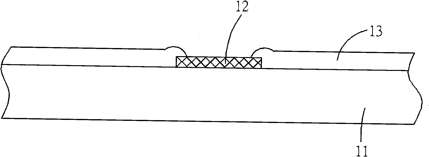
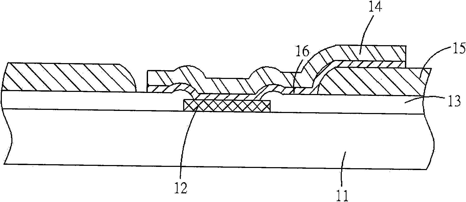
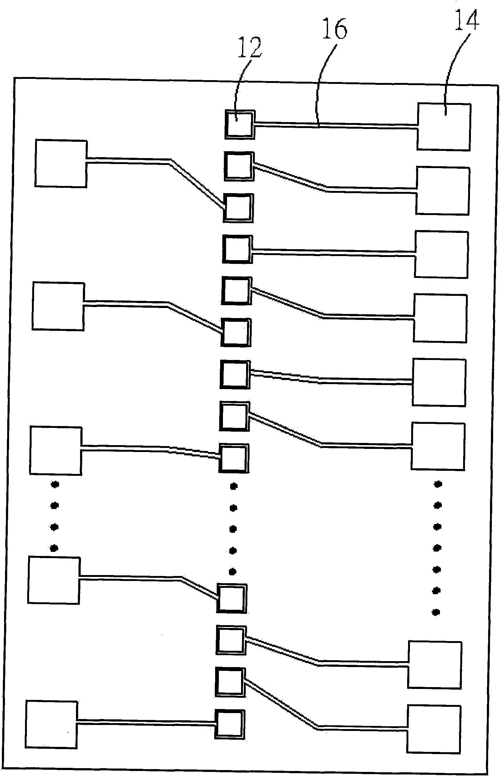
[0035] The stress-reducing dielectric layer structure and its manufacturing method of the present invention, the structure of the integrated circuit assembly 21 is as follows Figure 4 As shown, the integrated circuit component 21 is provided with a welding pad 22, a protective layer 23 and a first dielectric layer 24, the protective layer 23 covers the surface of the integrated circuit component 21, and the first dielectric layer 24 covers the protective layer. layer 23 surface, the protective layer 23 is provided with a first window 231 to expose the pad 22, and the first dielectric layer 24 is also provided with a second window 241 to expose the pad 22, the first and second windows 231 , 241 overlap up and down, and the size of the windows may be the same or different. In the embodiment shown in the figure, the opening ratio ...


PUM


Abstract

The invention relates to a dielectric layer structure for reducing stress and a manufacturing method thereof. An integrated circuit component is provided with a weld pad, a protective layer and a first dielectric layer, wherein the protective layer is covered on the surface of the integrated circuit component; the first dielectric layer is covered on the surface of the protective layer; the protective layer and the first dielectric layer enable the weld pad to be exposed; the first dielectric layer is provided with a reconfigured weld pad connected with the weld pad through an under bump metal layer (UBM), a subsequent electroplated metal layer and an original weld pad; a plurality of through grooves are formed on the first dielectric layer, and each through groove passes through the upper surface and the lower surface of the first dielectric layer and divides the first dielectric layer into a plurality of blocks. The shrinkage stress generated after curing of the first dielectric layer is reduced by utilizing the discontinuous blocks, and the heat expansion of the first dielectric layer is buffered through each through groove so as to prevent crystal grains bending after wafer is thinned and cut.

Description

technical field [0001] The present invention relates to a stress-reducing dielectric layer structure and its manufacturing method, aiming at reducing the shrinkage stress of the first dielectric layer after curing, so as to prevent the dielectric layer from wafer thinning and crystal grain bending after cutting structure and method of manufacture. Background technique [0002] In the semiconductor industry, the production of integrated circuits is mainly divided into three stages: the manufacture of silicon grains, the manufacture of integrated circuits, and the packaging of integrated circuits. The packaging of integrated circuits is the final step in the completion of finished integrated circuits. The purpose of the package is to provide a medium for electrical connection between the die and a printed circuit board (PCB) or other components, and to protect the die. [0003] After the semiconductor manufacturing process is completed, the die is formed by dicing the wafer....

Claims


Application Information

Patent Timeline
Patent Type & Authority Applications(China)
IPC IPC(8): H01L23/485H01L21/60
CPCH01L24/06H01L2224/02166H01L2224/05554H01L2924/14
Inventor 陆颂屏黄昆永刘国雄陈孟祺
Owner FUPO ELECTRONICS CORP
Why Eureka
Try Eureka