Electrostatic discharge testing circuit and correlated method thereof

A technology of electrostatic discharge detection and electrostatic discharge, applied to circuits, emergency protection circuit devices for limiting overcurrent/overvoltage, circuit devices, etc., can solve leakage current generation, false start, and inverting circuit 220 cannot be effectively Closing and other issues

Active Publication Date: 2009-12-09
FARADAY TECH CORP
View PDF0 Cites 17 Cited by
  • Summary
  • Abstract
  • Description
  • Claims
  • Application Information

AI Technical Summary

Problems solved by technology

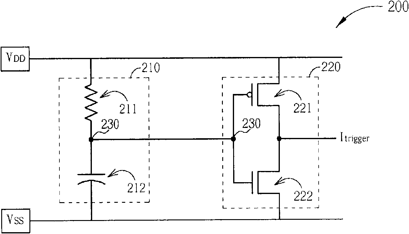
[0007] However, when utilizing the metal oxide layer capacitance formed by the advanced process (nano scale process), the thinner thickness of the gate oxide layer tends to cause serious leakage current in the static electricity detection circuit, which may make the static electricity The discharge protection circuit produces a malfunction (malfunction), which makes it unable to achieve its normal logic under normal working conditions, resulting in a more serious leakage current
[0008] The leakage current phenomenon of the electrostatic protection circuit is caused by the capacitive resistance circuit of the electrostatic discharge detection circuit (refer to figure 2 The metal oxide semiconductor transistor capacitor 212 in ) adopts an advanced process thin oxide layer component. At this time, a large amount of tunneling current (tunneling current) often occurs at the gate terminal of the metal oxide semiconductor transistor capacitor 212, which causes the chip to fail normally. During operation, the voltage of a connection terminal between the capacitive resistance circuit 210 and the inverter circuit 220 (which is coupled to a control terminal of the PMOS transistor 221 and a control terminal of the NMOS transistor 222) is relatively The voltage value of a first connection terminal (which is coupled to the first power supply pad) of the PMOS transistor 221 is a relatively low voltage, so the PMOS transistor is turned on. while causing electrostatic discharge to trigger the signal I trigger Transition from a low logic level to a high logic level, thus falsely enabling subsequent ESD protection components (such as power supply clamping circuits)
In other words, when the ESD event does not occur, the tunneling current of the metal oxide semiconductor transistor capacitor 212 will pull down the voltage value of the connection terminal 230 (which connects the capacitive resistance circuit 210 and the inverter circuit 220 ), thus causing The inverter circuit 220 cannot be effectively turned off under normal operation of the chip, resulting in a large amount of leakage current generated between the two power supply pads (between the VDD terminal and the VSS terminal)

Method used


Image

  • Electrostatic discharge testing circuit and correlated method thereof
  • Electrostatic discharge testing circuit and correlated method thereof
  • Electrostatic discharge testing circuit and correlated method thereof

Examples


Embodiment Construction

[0040] Certain terms are used throughout the specification and appended claims to refer to particular elements. Those skilled in the art should understand that manufacturers may use different terms to refer to the same component. This specification and the appended claims do not use the difference in name as a way to distinguish components, but use the difference in function of components as a criterion for distinguishing. The "comprising" mentioned throughout the specification and subsequent claims is an open term, so it should be interpreted as "including but not limited to". Otherwise, the term "coupled" includes any direct and indirect means of electrical connection. Therefore, if it is described that a first device is coupled to a second device, it means that the first device may be directly electrically connected to the second device, or indirectly electrically connected to the second device through other devices or connection means.

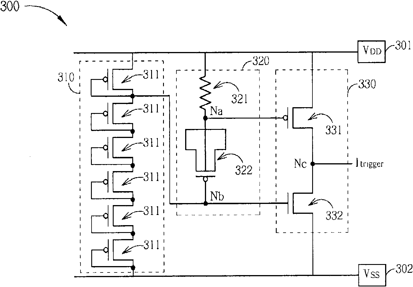
[0041] see image 3 , image 3 ...


PUM


Abstract

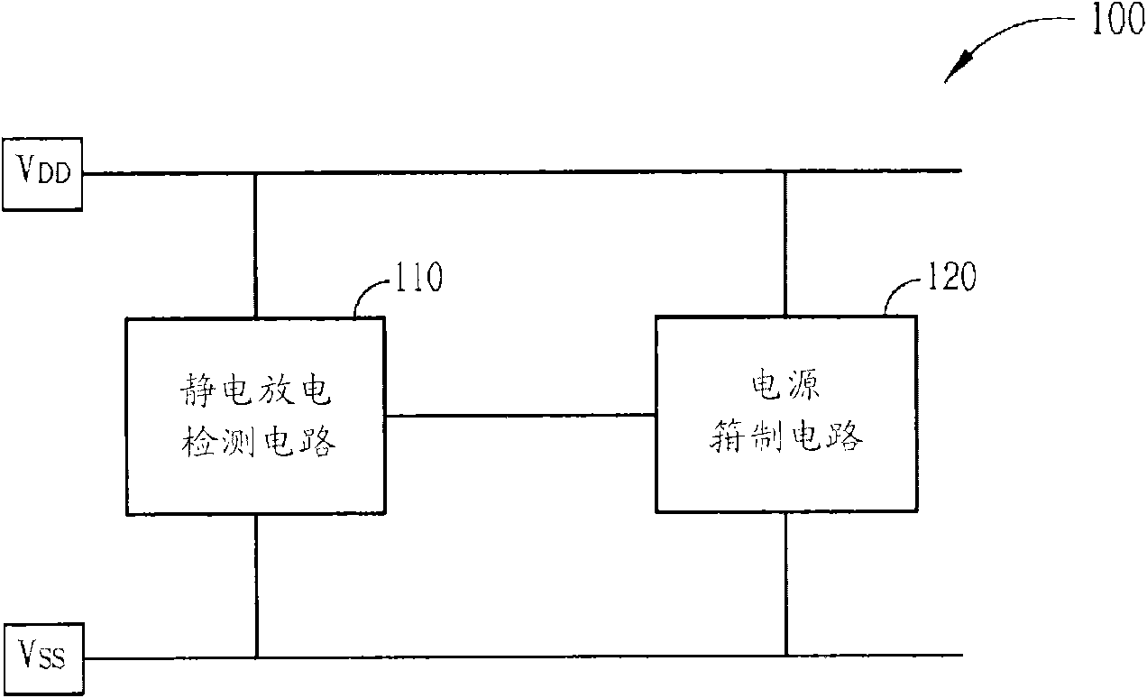
The invention relates to an electrostatic discharge testing circuit and a correlated method thereof. The electrostatic discharge testing circuit comprises a first power source bonding pad, a second power source bonding pad, an RC circuit, a trigger circuit and a bias circuit, wherein the RC circuit comprises a resistor element and a capacitor element; the first power source bonding pad receives a first supply voltage; the second power source bonding pad is used for receiving a second supply voltage different from the first supply voltage; the resistor element is coupled between the first power source bonding pad and a first terminal, and the capacitor element is coupled between the first terminal and a second terminal; the trigger circuit is used for generating an electrostatic discharge triggering signal according to a voltage level between the first terminal and the second terminal; and the bias circuit is used for supplying a bias voltage to the second terminal.

Description

technical field [0001] The present invention relates to electrostatic discharge protection (ESD protection), in particular to an electrostatic discharge detection (ESD detection) circuit and a related method applied to an electrostatic discharge protection circuit using advanced process components. Background technique [0002] With the advancement of science and technology, the process technology of integrated circuits has also been continuously improved. As known to those skilled in the art, various electronic circuits can be integrated / formed on a chip, and in order to enable the chip to receive an external voltage source (such as a bias power supply) and exchange data with other external circuits / chips, Conductive pads are provided on the chip. For example, in order to transmit the bias voltage, a power pad may be provided on the chip. In addition, signal pads (signal pads), ie input / output pads (I / O pads), are also provided on the chip for receiving input signals and / ...

Claims


Application Information

Patent Timeline
Patent Type & Authority Applications(China)
IPC IPC(8): H01L27/02H02H9/00G01R31/00
Inventor 柯明道邱柏砚黄俊
Owner FARADAY TECH CORP
Why Eureka
Try Eureka