Light emitting diode (LED) chip with vertical structure adopting electric conduction polymer transferring and manufacturing method thereof

A conductive polymer and LED chip technology, applied in semiconductor/solid-state device manufacturing, circuits, electrical components, etc., can solve the problems of unfavorable slicing process and inability to manufacture vertical structures, etc., achieve easy slicing process, solve heat dissipation and light blocking, The effect of improving compound efficiency

Inactive Publication Date: 2009-12-09
GUANGDONG REAL FAITH OPTO
View PDF0 Cites 23 Cited by
  • Summary
  • Abstract
  • Description
  • Claims
  • Application Information

AI Technical Summary

Problems solved by technology

In the wafer bonding process, metals and insulating transparent polymers are mainly used as bonding materials at present, but the use of these materials as bonding layers has the following problems: (1) the us

Method used


Image

  • Light emitting diode (LED) chip with vertical structure adopting electric conduction polymer transferring and manufacturing method thereof
  • Light emitting diode (LED) chip with vertical structure adopting electric conduction polymer transferring and manufacturing method thereof
  • Light emitting diode (LED) chip with vertical structure adopting electric conduction polymer transferring and manufacturing method thereof

Examples


Embodiment Construction

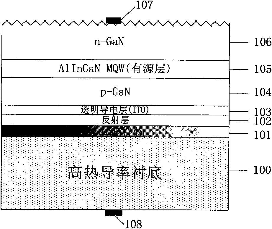
[0028] In the following, only silicon (Si) is used as a substrate with high thermal conductivity as an example for description.

[0029] The method for preparing a vertical structure LED chip and the structure of the chip by using a conductive polymer with high thermal conductivity as a bonding layer will be described in detail below with reference to the accompanying drawings of the present invention.

[0030] figure 1 It is a cross-sectional view of a vertical structure LED chip bonded with a conductive polymer, and the following is combined with the attached figure 1 The structure and characteristics of the vertical structure LED chip prepared on the silicon substrate according to the present invention will be described in detail.

[0031] (1) High thermal conductivity substrate (100), used as the substrate of the vertical structure LED chip.

[0032] (2) Conductive polymer (101) is above the high thermal conductivity substrate, reflective layer (102), is ITO transparent ...


PUM

PropertyMeasurementUnit
Thicknessaaaaaaaaaa
Thicknessaaaaaaaaaa
Thermal conductivityaaaaaaaaaa

Abstract

The invention discloses a light emitting diode (LED) chip with a vertical structure adopting electric conduction polymer transferring and a manufacturing method thereof, the method has the following steps: evaporating an ITO transparent conductive layer on the LED epitaxial wafer of a sapphire substrate; evaporating Al, Ag or Pt as a reflecting layer on the transparent conductive layer; coating conductive adhesive with high heat conductivity on the reflecting layer; bonding the LED epitaxial wafer on the high heat conductivity substrate by the conductive adhesive; adopting inductively coupled plasma (ICP) or reactive ion etching (RIE) n-GaN, an active layer and p-GaN; etching off the undoped GaN layer by adopting KOH solution and coarsing the n-GaN surface; evaporating n side electrode and p side electrode. The proposal improves the heat dissipation efficiency of products and the comprehensive performance of the LED chip.

Description

technical field [0001] The invention relates to a method for preparing a GaN-based power light-emitting diode (LED) chip with a vertical structure, in particular to a method for transferring a GaN-based LED epitaxial wafer on a sapphire substrate to a material with high thermal conductivity by using a high thermal conductivity and conductive polymer , preparing an LED chip with an upper and lower electrode structure and a preparation method thereof. Background technique [0002] GaN-based blue and blue-green light-emitting diodes (LEDs) are widely used in instrument indicators, large-size LED backlights, electronic billboards, and various lighting equipment. Due to the limitations of GaN crystal structure and growth conditions, sapphire is mainly selected as the substrate when growing GaN-based LED epitaxial layers. Due to the poor electrical and thermal conductivity of sapphire, the manufacturing process of GaN-based LEDs is complicated, the heat dissipation is poor, and t...

Claims


Application Information

Patent Timeline
IPC IPC(8): H01L33/00H01L21/78
Inventor 刘胜甘志银王凯汪沛周圣军金春晓
Owner GUANGDONG REAL FAITH OPTO
Why Eureka
Try Eureka