

Semiconductor laser TO tube seat packaging beam compression process
A technology of lasers and semiconductors, applied in the direction of semiconductor lasers, lasers, devices for controlling output parameters of lasers, etc., can solve problems such as uncertainty, material waste cost, and complex compression process, so as to avoid grinding, simplify process steps, and shape the process The effect of improving efficiency
- Summary
- Abstract
- Description
- Claims
- Application Information
AI Technical Summary
Problems solved by technology
Method used
Image

Examples
Embodiment Construction
[0015] The beam compression process of the present invention is as figure 1 As shown, the specific process is as follows:
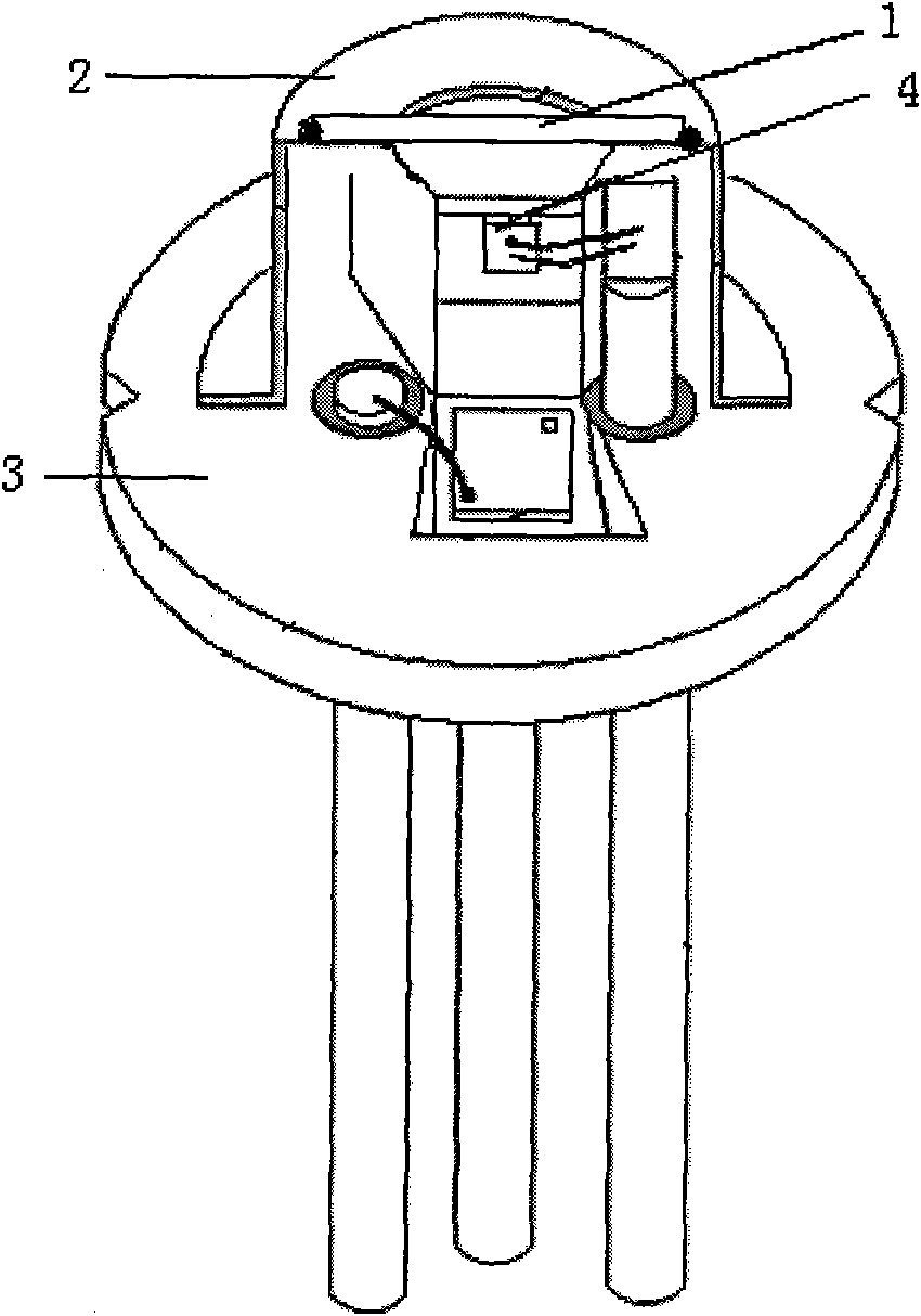
[0016] The TO socket 3 adopts an existing common structure, including a shell, a nozzle and a pin, and the shape of the nozzle is a hexagonal column. First, solder is evaporated on the tongue as usual, and then the chip of the semiconductor laser is bonded in the middle of the tongue, so that the surface of the light-emitting cavity of the chip is flush with the upper surface of the tongue, and then the alloy is carried out at 180°C, and the bond is carried out after the alloy Hehe Optoelectronics Testing.
[0017] Then use the tube cap 2 corresponding to the model of the TO tube base 3 to package the tube cap 2 on the TO tube base 3, and the tube cap 2 is in the middle of the tube base 3, that is, the centerline of the tube cap coincides with the centerline of the tube base.
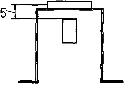
[0018] Adhesive cylindrical lens 1 on the outside of tube cap 2, such as f...
PUM
 Abstract
Description
Claims
Application Information