

Method for manufacturing large-scale integrated circuit lead frame
A large-scale integrated circuit lead and lead frame technology, which is applied in the direction of circuit, semiconductor/solid-state device manufacturing, electrical components, etc., can solve the problems of coplanarity and low qualified rate of displacement index, so as to avoid hooking dislocation deformation, The effect of novel concept and enhanced pin rigidity
Active Publication Date: 2011-01-05
NINGBO HUALONG ELECTRONICS
View PDF0 Cites 0 Cited by
- Summary
- Abstract
- Description
- Claims
- Application Information
AI Technical Summary
Problems solved by technology
The technical problem to be solved by the present invention is to overcome the defects and deficiencies of the existing large-scale integrated circuit lead frame pin coplanarity and low displacement index pass rate, and provide the society with a high production efficiency, stable finished product quality, qualified A high-efficiency large-scale integrated circuit lead frame manufacturing method to meet the needs of subsequent large-scale integrated circuit packaging process applications
Method used
View moreImage
Smart ImageViewing Examples

Examples
Embodiment Construction
Login to View More PUM
 Abstract
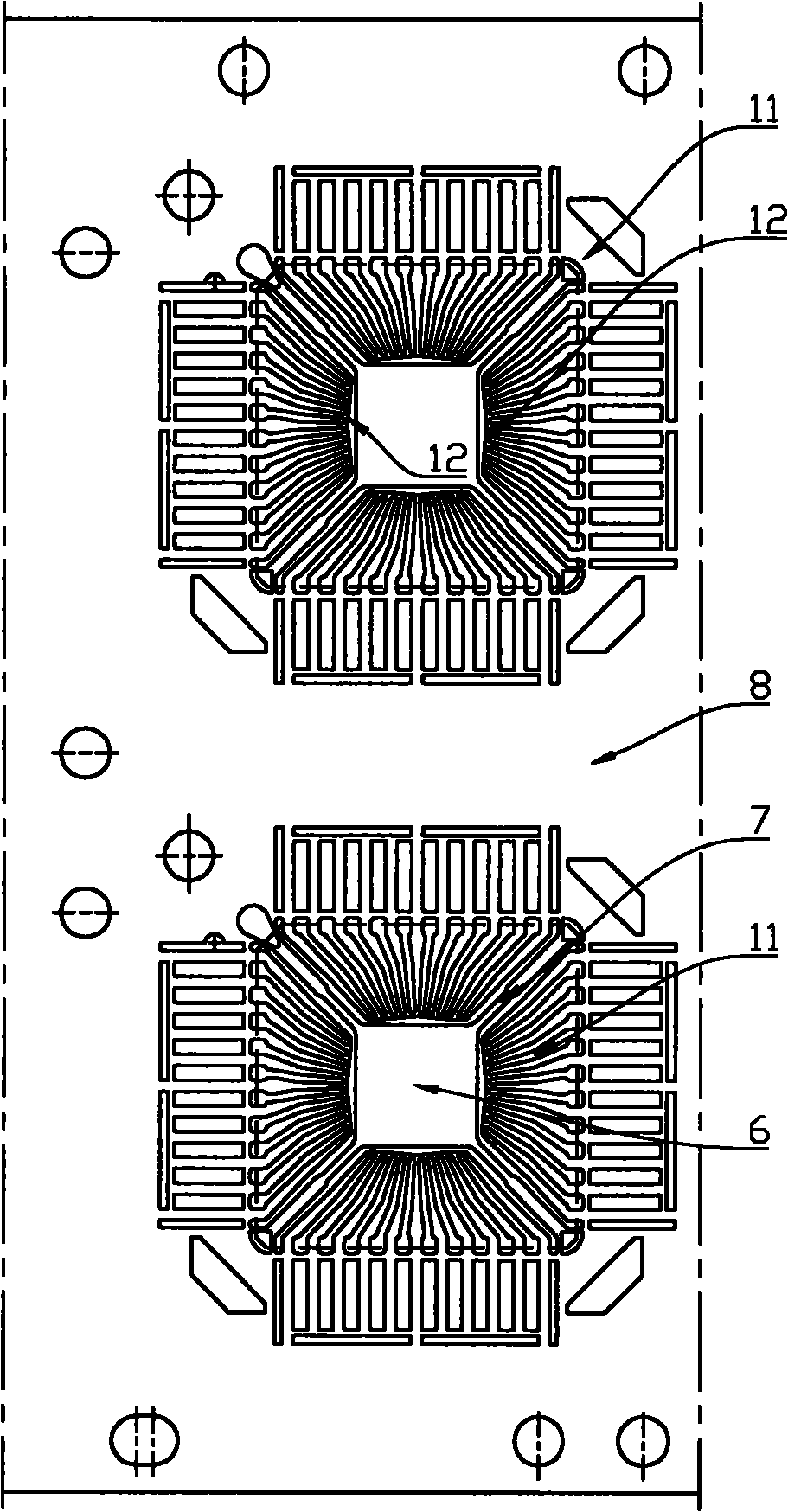
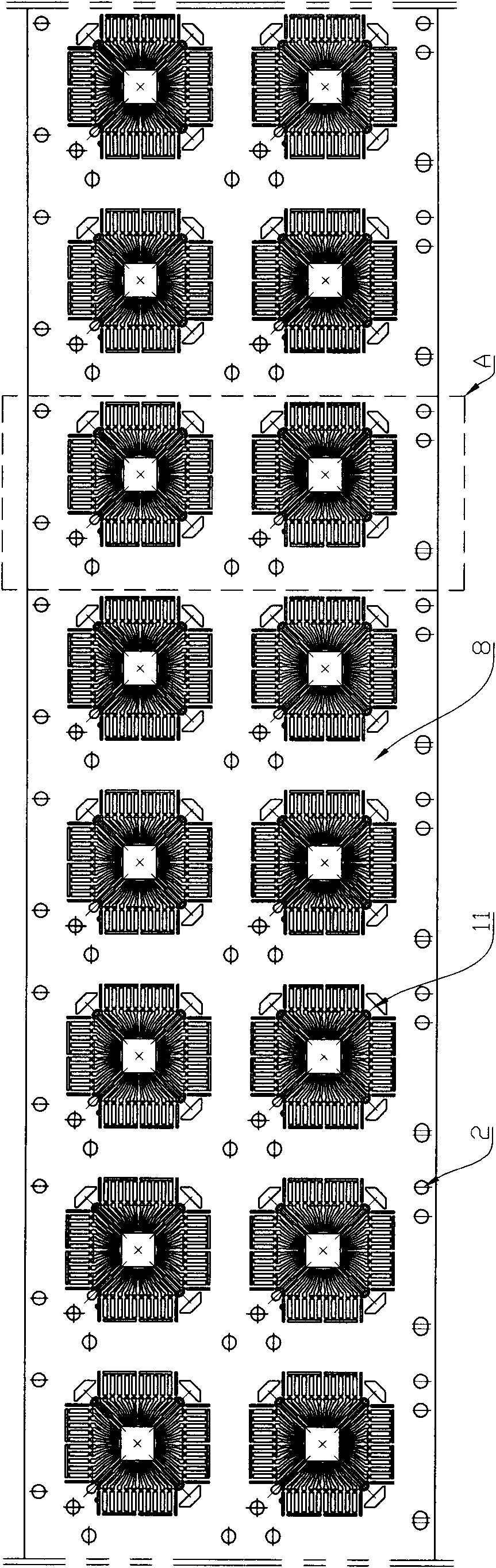
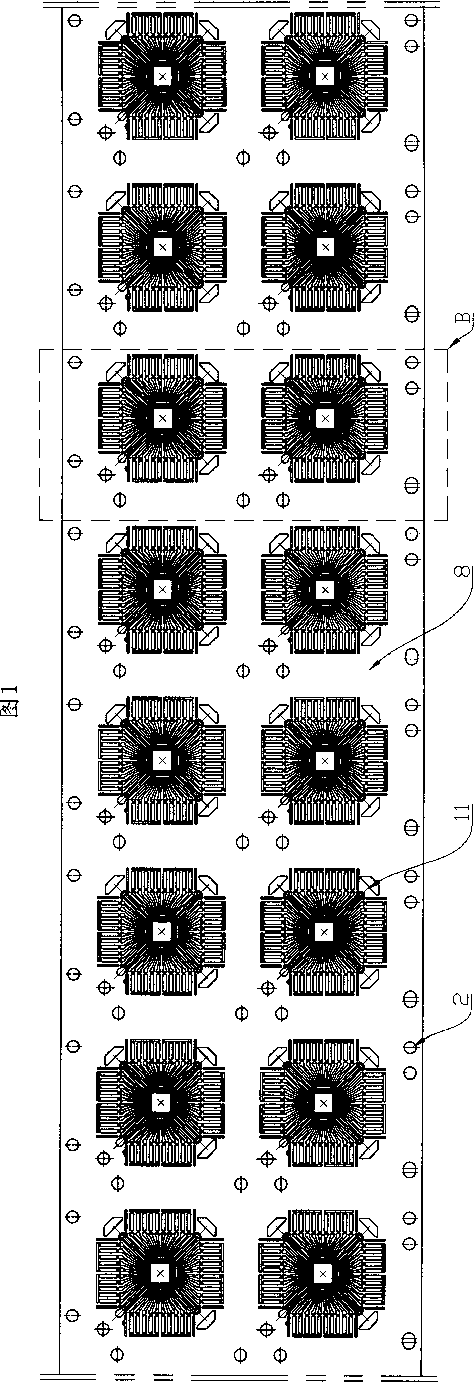
The invention discloses a method for manufacturing a large-scale integrated circuit lead frame, which overcomes the defect of lower index qualification rate of the coplanarity and the displacement of pins of a lead frame manufactured in the prior art. The method comprises the following steps: (1) continuously stamping: continuously stamping a zone ring with a lead frame original blank on a die; (2) continuously electroplating: electroplating the zone ring with the lead frame original blank, wherein the electroplating area comprises the root welding area of the pins and the front surface of the chip island; and (3) slicing and confirming the size: cutting and flaking the electroplated zone ring to obtain a single plate lead frame piece, wherein in the step of continuous stamping, a connecting rib for connecting the end parts of a plurality of pins at each side into a whole is retained at one end of the pins in the lead frame original blank approaching to the four sides of the chip island, and in the step of slicing and confirming the size, when the zone ring is cut and the size is confirmed, the connecting rib of the end parts of the pins approaching to the four sides of the chip island is also cut off to obtain a finished lead frame. The invention can greatly improve the qualification rate of the coplanarity and the displacement of the pins of the finished lead frame.
Description
A kind of manufacturing method of large-scale integrated circuit lead frame technical field The invention relates to a manufacturing technology of a lead frame product for semiconductor microelectronic packaging, in particular to a manufacturing method of a stamping type lead frame. Background technique With the rapid development of science and technology, especially the rapid development of semiconductor microelectronics intelligent technology, large-scale integrated circuit components are increasingly showing the industry development trend of miniaturization, thinning and integration. The IC lead frame parts of the basic components of large-scale integrated circuits are becoming thinner and thinner. The number of pins on the periphery of the chip island ranges from more than ten to as many as dozens. The difficulty of processing and manufacturing is far greater than that of ordinary triodes. Lead frame products. As we all know, the existing manufacturing methods of lead...
Claims
Login to View More Application Information
Patent Timeline
 Patent Type & AuthorityPatents(China)
IPC IPC(8): H01L21/48H01L23/495
CPCH01L2924/0002
Inventor陈孝龙陈明明李靖朱敦友
OwnerNINGBO HUALONG ELECTRONICS