Platy LED metal substrate, platy LED light emitting device and manufacturing method thereof

A technology for metal substrates and light-emitting devices, which can be used in semiconductor/solid-state device manufacturing, electrical components, and electrical solid-state devices, etc., and can solve problems such as deformation

Active Publication Date: 2010-01-20
FOSHAN NATIONSTAR OPTOELECTRONICS CO LTD
View PDF2 Cites 11 Cited by
  • Summary
  • Abstract
  • Description
  • Claims
  • Application Information

AI Technical Summary

Problems solved by technology

[0005] An object of the present invention is to provide a chip-type LED metal substrate, which can overcome the problem of easy deformation in the prior art. The substrate of the present invention has two upper hole parts and lower hole parts opposite to each other. A lead connection part connected to the inner side of the upper hole and the lower hole, a chip placement part connected to the lead connection part connected to the upper hole, two welding parts respectively connected to the outer side of the upper hole and the lower hole, and Two reinforcement ribs located on both sides of the chip placement part and connecting the upper hole part and the lower hole part

Method used


Image

  • Platy LED metal substrate, platy LED light emitting device and manufacturing method thereof
  • Platy LED metal substrate, platy LED light emitting device and manufacturing method thereof
  • Platy LED metal substrate, platy LED light emitting device and manufacturing method thereof

Examples


Embodiment Construction

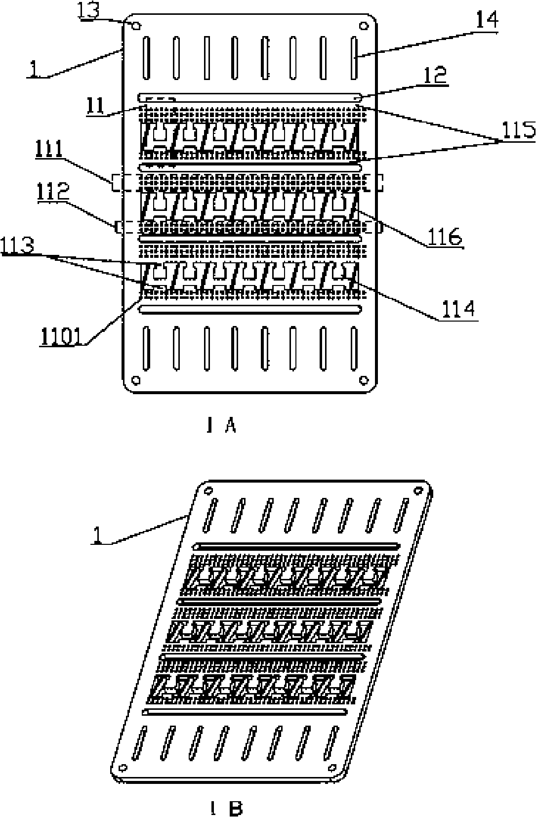
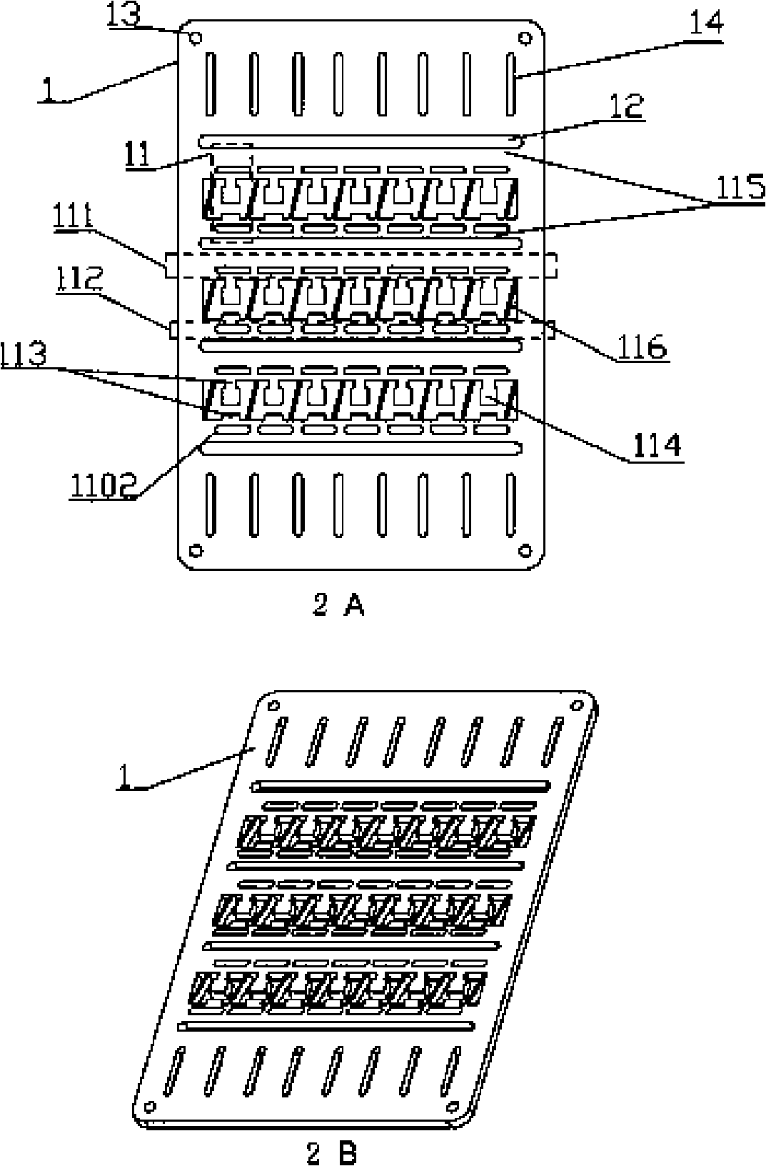
[0017] According to the above attached figure 1 And attached figure 2 , the packaging structure and manufacturing method of the chip LED lighting device of the present invention will be further described.

[0018] In this embodiment, the structure of the metal substrate 1 of the present invention includes a substrate unit array of M rows×N columns, wherein M and N are at least equal to 1 at the same time, and separation groove lines are set on both sides of each substrate unit row, totaling M+ 1, separate each substrate unit row, and N+1 cutting reference holes are respectively provided at both ends of the substrate unit row, corresponding to the side of each substrate unit row; as attached figure 1 , 2 The structure of the metal substrate 1 shown includes: an array of substrate units 11 in 3 rows×7 columns, 4 dividing groove lines 12 , 4 positioning holes 13 and 16 cutting reference holes 14 .

[0019] as attached figure 1 , attached figure 2 , attached Figure 5 The ...


PUM


Abstract

The invention relates to a platy LED metal substrate, a platy LED light emitting device and a manufacturing method thereof. The substrate is formed by elementary units which are provided with an upper hole part and a lower hole part opposite to each other, two lead connecting parts respectively connected with the inner sides of the upper hole part and the lower hole part, a chip placing part connected with the lead connecting part in connection with the upper hole part, two welding parts respectively connected with the outer sides of the upper hole part and the lower hole part, and two reinforcing ribs respectively located at two sides of the chip placing part and connected with the upper hole part and the lower hole part. The invention also relates to a method for manufacturing the platy LED light emitting device, comprising the steps of die cutting metal substrate, plating, printing ink, placing LED chip, bonding lead, packaging stamp, cutting wafer saw and testing package. The invention also relates to the metal substrate and a platy LED light emitting device manufactured by the method. The invention is simple in the process and improves the consistency and reliability of products; in addition, the manufactured platy LED light emitting device is featured by excellent performance and favorable consistency.

Description

technical field [0001] The patent of the present invention relates to a light-emitting diode (LED) technology, in particular to a chip-type LED metal substrate, a chip-type LED light-emitting device and a manufacturing method thereof. Background technique [0002] With the continuous improvement of LED production technology and the continuous expansion of LED application range, the requirements for LED brightness and photoelectric stability are continuously improved. At present, the production technology of chip light emitting diodes is quite mature. For example, the Chinese patent application number is 01131330.7, and the application date is April 10, 2002. The name of the invention is chip light emitting diodes and its manufacturing method. A base on one side, a body part extending from the base and arranged through a hole provided on the main printed circuit board, a light emitting part provided on the main body part and emitting light on the other side of the main printe...

Claims


Application Information

Patent Timeline
Patent Type & Authority Applications(China)
IPC IPC(8): H01L33/00H01L21/50H01L25/075
CPCH01L24/97H01L2924/01033H01L2924/01005H01L2924/01006H01L2924/01029H01L2924/01082H01L2924/01047H01L2924/01079H01L2224/48091H01L2224/48465H01L2224/97H01L2924/12041H01L2224/73265
Inventor 余彬海李军政潘利兵梁丽芳龙孟华
Owner FOSHAN NATIONSTAR OPTOELECTRONICS CO LTD
Why Eureka
Try Eureka