A method of forming a circuit structure

A circuit structure and manufacturing method technology, applied in nanostructure manufacturing, circuits, semiconductor/solid-state device manufacturing, etc., can solve the problems of GaN film cracking, GaN film 15 cracking, bad effects, etc. The effect of sorting and improving quality

Active Publication Date: 2010-02-17
TAIWAN SEMICON MFG CO LTD
View PDF0 Cites 3 Cited by
  • Summary
  • Abstract
  • Description
  • Claims
  • Application Information

AI Technical Summary

Problems solved by technology

This may have some adverse effects
First, a large number of defects (dislocation) may be generated in the crystalline GaN film
Second, the thickness uniformity of the formed GaN film is low, which causes the wavelength shift (wavelength shift) of the light emitted by the optical element formed on the GaN film
Third, GaN films with large stresses can generate cracks
[0007] However, the above manufacturing process has disadvantages
Since the nanostructures 11 and 12 need to be formed under optimized manufacturing process conditions, it is difficult to control the size, pattern density and uniformity of the nanostructures 11 and 12
This affects the thickness uniformity of the formed GaN film 15
In addition, the nanostructures in this example have an undesirably large width, thus requiring a large mechanical force to separate the GaN film from the sapphire substrate 10
This not only causes more dislocations to be formed in the GaN film 15, but also breaks the generally very thin GaN film 15.

Method used


Image

  • A method of forming a circuit structure
  • A method of forming a circuit structure
  • A method of forming a circuit structure

Examples


Embodiment Construction

[0033] The manner in which the various embodiments can be made and used are described in detail below. However, it is worth noting that the various applicable inventive concepts provided by the present invention are implemented according to various changes in the specific text, and the specific embodiments discussed here are only used to show the specific use and manufacture of the present invention. method of invention, but not to limit the scope of the invention.

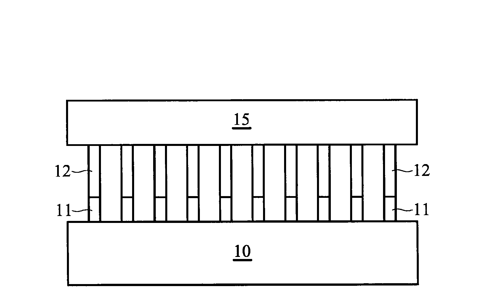
[0034] The present invention provides a method of forming a Group III nitride (hereinafter referred to as III nitride) semiconductor film and a formed structure. The manufacturing process of the preferred embodiment of the present invention is described below through various diagrams and examples. In addition, the same symbols represent the same or similar elements in various different embodiments and illustrations of the present invention.

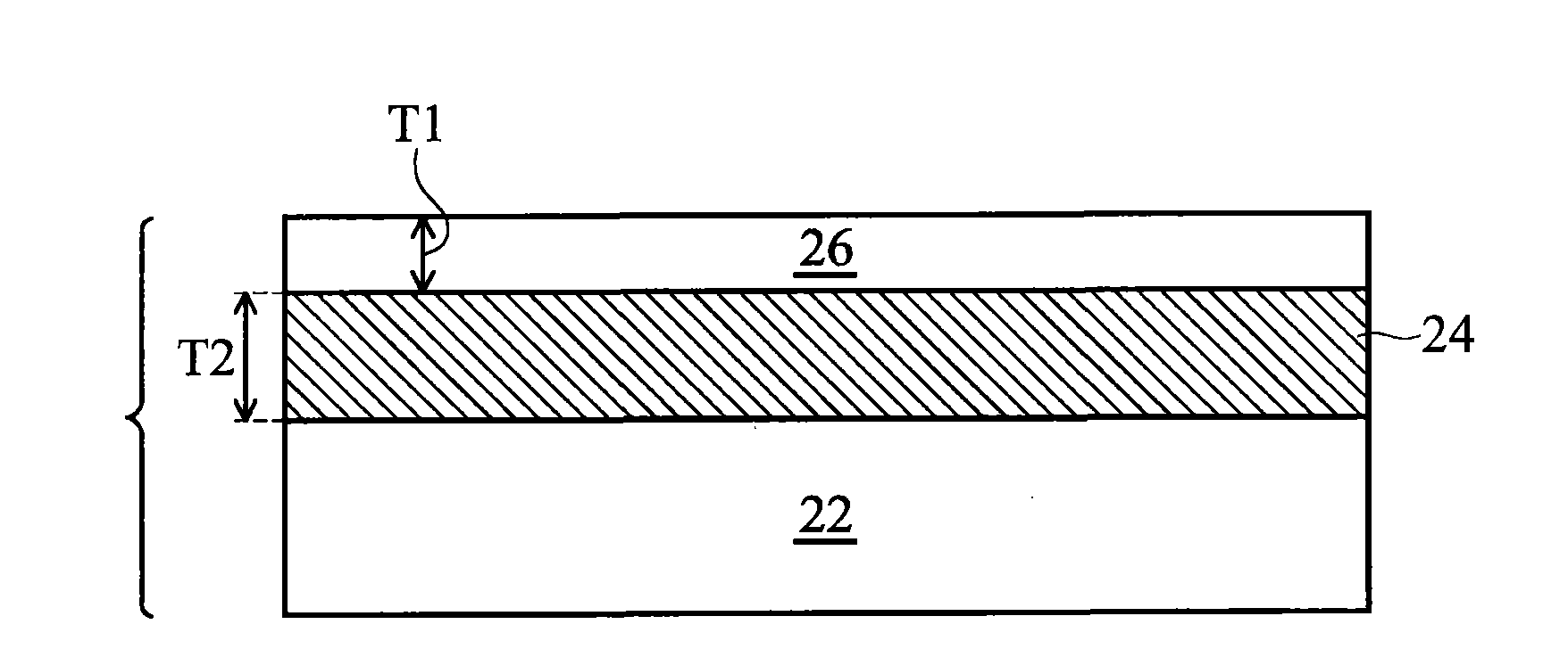
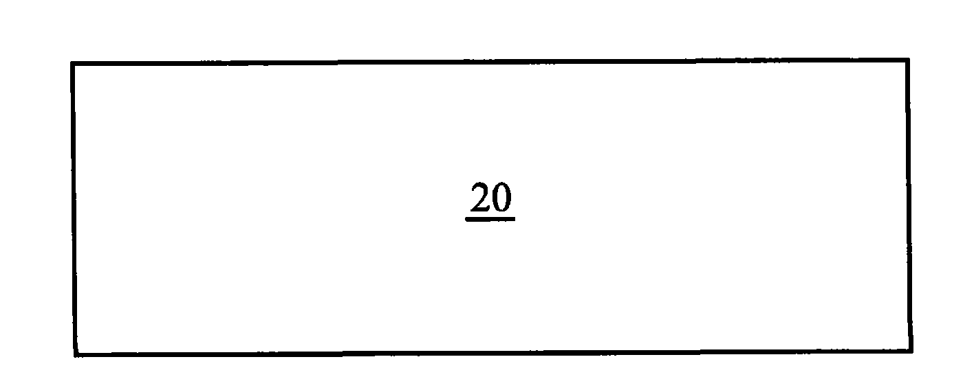
[0035] Figure 2A and Figure 2B Substrate 20 is shown. Please refe...


PUM

PropertyMeasurementUnit
thicknessaaaaaaaaaa
thicknessaaaaaaaaaa
thicknessaaaaaaaaaa

Abstract

A method of forming a circuit structure includes providing a substrate; etching the substrate to form a plurality of nano-structures; and growing a compound semiconductor material onto the nano-structures using epitaxial growth. Portions of the compound semiconductor material grown from neighboring ones of the nano-structures join each other to form a continuous compound semiconductor film. The present invention can accurately control the size of the nano column, the pattern density and the uniformity, thus causing the III-nitride film to have an improved quality formed thereon; causing obviously transverse growth to reduce the dislocation in the III-nitride film; causing the torque force required by the nano column breakage to be samll; and ensuring that the nano column portion is a portion having weak mechanical strength, which can be easily broken or etched.

Description

technical field [0001] The present invention relates to a method of manufacturing a semiconductor device, and more particularly to a method of manufacturing a Group III nitride film. Background technique [0002] In recent years, since group-III nitride (commonly referred to as III-nitride or III-nitrogen (III-N)) compounds, such as gallium nitride (GaN) and its related Alloys are actively studied for their promising applications in electronic or optoelectronic components. Specific examples of possible optoelectronic elements include blue light emitting diodes and laser diodes, and ultra-violet photo-detectors. The high energy gap and high electron saturation velocity (electron saturation velocity) characteristics of III nitrogen compounds also make them an excellent choice in the application of high temperature and high speed power electronic components. [0003] Since the equilibrium pressure of nitrogen element (nitrogen) is high at a general growth temperature, it is d...

Claims


Application Information

Patent Timeline
Patent Type & Authority Applications(China)
IPC IPC(8): H01L21/20B82B3/00
CPCH01L21/02639H01L21/02603H01L21/02422H01L21/0245H01L21/0265H01L21/0254H01L21/02381
Inventor 陈鼎元邱文智余振华
Owner TAIWAN SEMICON MFG CO LTD
Why Eureka
Try Eureka