Method for manufacturing large-diameter silicon wafer

A manufacturing method and large-diameter technology, applied in semiconductor/solid-state device manufacturing, electrical components, circuits, etc., can solve problems affecting processing speed, etc., achieve the effects of increasing productivity, reducing polishing time, and ensuring processing accuracy

Inactive Publication Date: 2010-02-24
GENERAL RESEARCH INSTITUTE FOR NONFERROUS METALS BEIJNG +1
View PDF0 Cites 15 Cited by
  • Summary
  • Abstract
  • Description
  • Claims
  • Application Information

AI Technical Summary

Problems solved by technology

However, during the grinding process of the silicon wafer, due to the rigid removal of the diamond grit and the surface of the silicon wafer, an oxide layer will be generated locally at high temperature, and the existence of the surface oxide layer will affect the processing speed of the next step.

Method used


Image

  • Method for manufacturing large-diameter silicon wafer
  • Method for manufacturing large-diameter silicon wafer
  • Method for manufacturing large-diameter silicon wafer

Examples


Embodiment 1

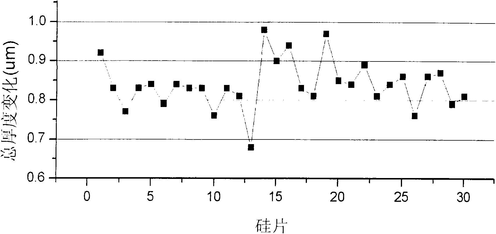
[0023] Use 30 12-inch slices of P (100) produced by the Czochralski method, grind the silicon wafer with a double-sided grinding machine, and use the AFS3220 geometric parameter tester to test the silicon wafer GBIR (the total thickness change of the silicon wafer) after grinding. To measure, the GBIR value of each piece is as figure 2 shown. It can be seen from the figure that the GBIR is less than 1 micron, with an average value of 0.839 micron.

Embodiment 2

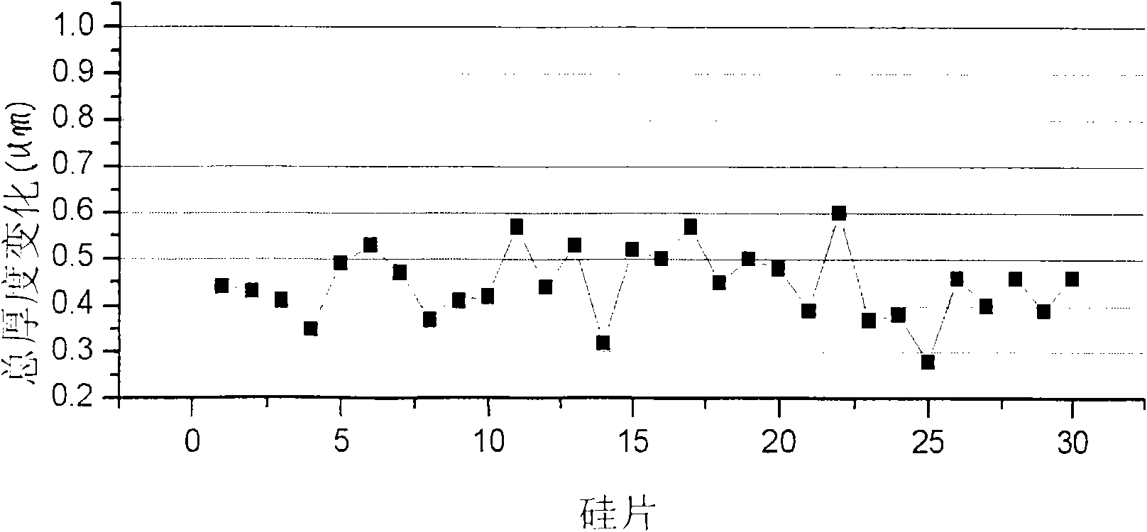
[0025] Get the above 30 silicon wafers through double-sided grinding, and use the method of the present invention to carry out double-sided polishing on a Speedfam20B polishing machine, and the polishing removal amount is 30 microns. Then wash it with a washing machine and dry it with a spin dryer. See GBIR after polishing. image 3 . It can be seen from the figure that the precision of the present invention is high, and the average value of GBIR is 0.459 microns, which are all less than 0.6 microns.


PUM


Abstract

The invention discloses a method for manufacturing a large-diameter silicon wafer, which comprises the following steps: (1) rinsing a ground silicon wafer with HF solution to remove an oxide layer onthe surface of the ground silicon wafer and improve the removal speed of double-side polishing; (2) performing conventional double-side polishing on the ground silicon wafer; and (3) performing single-side finishing polish and washing on the silicon wafer. The process method removes the oxide layer on the ground surface with the HF solution, better contributes to the double-side polishing, therebyreducing the polishing time greatly, reducing the removal amount of a silicon single crystal and improving the unit yield of the single crystal at the same time. Because of the reduction of a grinding amount and a corrosion amount, the method ensures machining accuracy of products powerfully, and can manufacture the large-diameter silicon wafer with high flatness. The method for manufacturing thelarge-diameter silicon wafer can be used for any technique for processing the large-diameter silicon wafer in commerce.

Description

technical field [0001] The present invention uses the improved large-diameter silicon wafer manufacturing process to process silicon polished wafers, specifically a method of rinsing silicon wafers with HF solution after double-sided grinding to remove the surface oxide layer, and then directly using conventional double-sided Polishing process for polishing. The silicon wafers processed by this processing technology can effectively reduce the processing time, and at the same time can improve the processing accuracy of the silicon wafers and the output rate of silicon single crystals. Background technique [0002] Semiconductor silicon wafer is the main substrate material of modern ultra-large-scale integrated circuits. Generally, it is an integrated circuit-level wafer manufactured through processes such as crystal pulling, slicing, chamfering, grinding (including grinding and grinding), corrosion, polishing, and cleaning. Semiconductor wafers. [0003] The ability of the ...

Claims


Application Information

Patent Timeline
Patent Type & Authority Applications(China)
IPC IPC(8): H01L21/00H01L21/02H01L21/302H01L21/304H01L21/306
Inventor 闫志瑞库黎明索思卓黄军辉葛钟陈海滨张国栋盛方毓
Owner GENERAL RESEARCH INSTITUTE FOR NONFERROUS METALS BEIJNG
Why Eureka
Try Eureka