Method for manufacturing QFN (quad flat no-lead) package device

A manufacturing method and a technology for packaging devices, which are applied in semiconductor/solid-state device manufacturing, electric solid-state devices, semiconductor devices, etc., can solve the problems of not being able to meet high density, limit the number of I/Os, increase packaging costs, etc., and achieve high I/O O density, high manufacturing precision, and the effect of eliminating air bubbles

Active Publication Date: 2013-04-03
南通腾龙通信科技有限公司
View PDF4 Cites 7 Cited by
  • Summary
  • Abstract
  • Description
  • Claims
  • Application Information

AI Technical Summary

Problems solved by technology

[0004] With the improvement of IC integration and the continuous enhancement of functions, the number of I/Os of ICs increases, and the number of I/O pins of corresponding electronic packages also increases accordingly. The pins of the ring are arranged around the chip carrier, which limits the increase in the number of I/Os and cannot meet the needs of high-density ICs with more I/Os.
Even if the traditional QFN package with non-step structure design has multi-turn pins, it cannot effectively lock the plastic packaging material, resulting in low bonding strength between the lead frame and the plastic packaging material, which is easy to cause delamination and even lead-out of the lead frame and plastic packaging material. The feet or the chip carrier fall off, and the moisture cannot be effectively prevented from diffusing into the electronic package along the interface between the lead frame and the plastic packaging material, which seriously affects the reliability of the package.
Even if the traditional QFN package has a stepped s

Method used


Image

  • Method for manufacturing QFN (quad flat no-lead) package device
  • Method for manufacturing QFN (quad flat no-lead) package device
  • Method for manufacturing QFN (quad flat no-lead) package device

Examples


Embodiment Construction

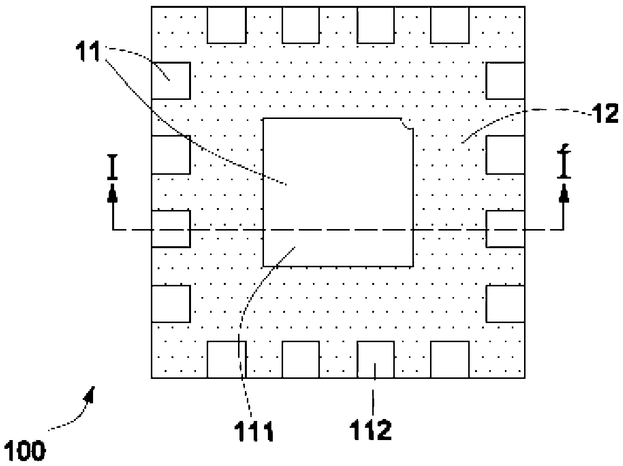
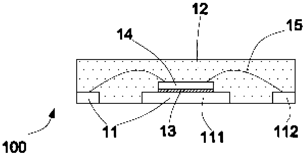
[0042] The present invention is described in detail below in conjunction with accompanying drawing:

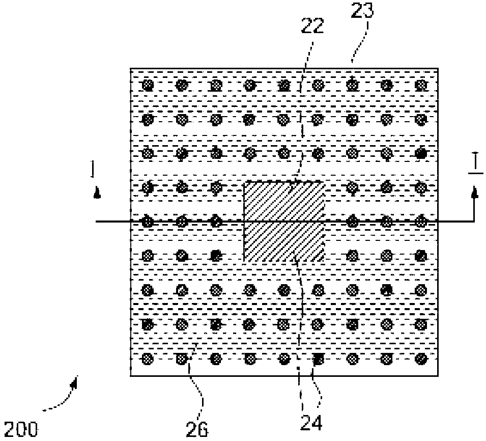
[0043] Figure 2A A schematic diagram of the back side of a multi-circle pin arrangement QFN packaged device drawn according to an embodiment of the present invention where the cross section of the pins is circular and the pins are arranged in parallel on each side of the chip carrier. Figure 2B A schematic diagram of the back side of a QFN packaged device in which the cross-section of the pins is rectangular and the pins on each side of the chip carrier are arranged in parallel according to the embodiment of the present invention.

[0044] Refer to the above Figure 2A-2B It can be seen that, in this embodiment, the QFN packaging device 200 with multi-circle pin arrangement has a chip carrier 22 and pins 23 arranged in multiple turns around the chip carrier 22, and the arrangement of the pins 23 on each side of the chip carrier 22 For parallel arrangement, a first metal ma...


PUM

PropertyMeasurementUnit
Thickness rangeaaaaaaaaaa
Thicknessaaaaaaaaaa

Abstract

The invention discloses a method for manufacturing a QFN (quad flat no-lead) package device. The chip load and pins of the manufactured QFN package device do not need to be based on a lead frame manufactured in advance, independent chip carriers and pins with step structures are formed by organically combining electroplating, mechanical grinding and cutting methods in a package technical process and are mechanically supported and protected by configured insulated filling materials in the package technical process, the insulated filling materials and plastic package materials are used for secondary coating and sealing, and the manufactured QFN package device has high I/O (input/output) density and fine reliability.

Description

technical field [0001] The invention relates to the technical field of manufacturing semiconductor components, in particular to a method for manufacturing a quadrilateral flat no-lead package with high I / O density. Background technique [0002] With the development of electronic products such as mobile phones and notebook computers towards miniaturization, portability, ultra-thinness, multimedia and low-cost requirements for popularization, high-density, high-performance, high-reliability and low-cost packaging forms and Its assembly technology has been developed rapidly. Compared with expensive BGA and other packaging forms, the new packaging technology developed rapidly in recent years, that is, Quad Flat Non-lead Package (QFN) package, has good thermal and electrical properties, small size, Many advantages such as low cost and high productivity have triggered a new revolution in the field of microelectronic packaging technology. [0003] Figure 1A and Figure 1B Respe...

Claims


Application Information

Patent Timeline
IPC IPC(8): H01L21/60H01L21/56
CPCH01L24/97H01L2224/32245H01L2224/48091H01L2224/48095H01L2224/48247H01L2224/48257H01L2224/73265H01L2224/97H01L2924/181H01L2924/00014H01L2924/00H01L2924/00012
Inventor 秦飞夏国峰安彤刘程艳武伟朱文辉
Owner 南通腾龙通信科技有限公司
Why Eureka
Try Eureka