Flexible OLED substrate and fabrication method thereof

A flexible, substrate-based technology, applied in the field of flexible OLED substrates and its preparation, can solve the problems of inability to meet OLED's requirements for the flatness of conductive film, unfavorable charge injection of OLED devices, short-circuit breakdown of devices, etc., to improve the uniformity of electric field performance, improve flatness, and reduce internal resistance and energy consumption

Inactive Publication Date: 2018-05-25
SUZHOU INST OF NANO TECH & NANO BIONICS CHINESE ACEDEMY OF SCI
View PDF7 Cites 9 Cited by
  • Summary
  • Abstract
  • Description
  • Claims
  • Application Information

AI Technical Summary

Problems solved by technology

[0004] When the transparent conductive layer of the existing metal grid is used in an OLED device with a thickness of only 100 nanometers, it is prone to uneven electric field and short-circuit breakdown of the device, which cannot meet the requirements of OLED for the flatness of the conductive film
Moreover, the work function of the existing transparent conductive layer is generally lower than 4.5eV, which is also very unfavorable to the charge injection of the OLED device.
In addition, OLED is extremely sensitive to water and oxygen in the air environment, and the water and oxygen permeability rate of the substrate is required to be lower than 10 ~6 g / m 2 / d, while the water oxygen transmission rate of the existing flexible transparent conductive layer substrate is 0.1g / m 2 / d above

Method used


Image

  • Flexible OLED substrate and fabrication method thereof
  • Flexible OLED substrate and fabrication method thereof
  • Flexible OLED substrate and fabrication method thereof

Examples


preparation example Construction

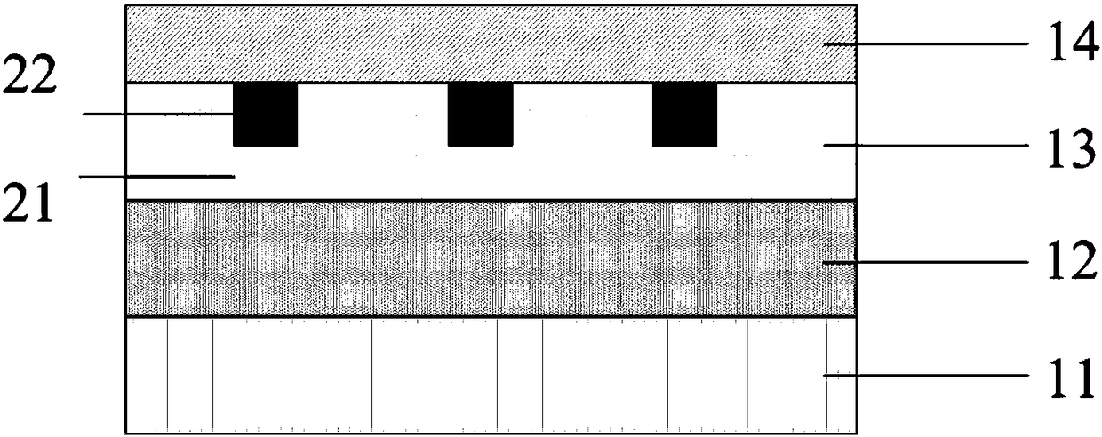
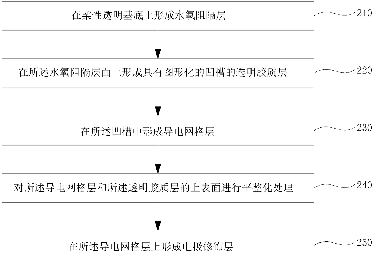
[0053] The embodiment of the invention also provides a preparation method of the flexible OLED substrate. refer to image 3 , the step of preparing a flexible OLED substrate specifically includes:

[0054] In step 210 , a water-oxygen barrier layer 12 is formed on the flexible transparent substrate 11 . Specifically, an organic / inorganic silicon hybrid high water oxygen barrier layer 12 is deposited on a flexible substrate by ICP-PECVD. Specifically, it is discharged by a high-density plasma source ICP source in a vertical direction, the sample is placed on the sample stage, the vacuum degree of the discharge deposition condition can be 0.1Pa-10Pa, and the discharge power of the ICP source can be 100W-1200W. Siloxane as precursor source, with O 2 , N 2 O, NH 3 Ar gas is used as the oxidizing gas source, and Ar gas is used as the auxiliary ionized gas source. By periodically adjusting the power of the ICP source and the different ratios of the precursor source and the oxid...

Embodiment 2

[0079] According to another embodiment of the present invention, a high temperature resistant flexible OLED substrate is also provided.

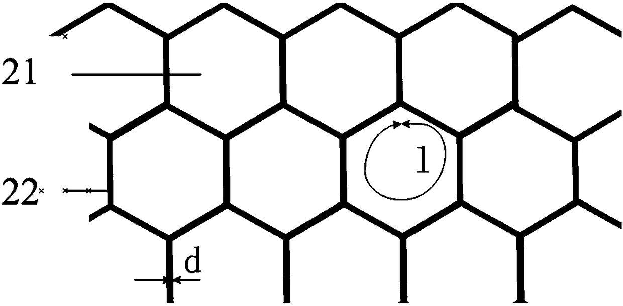
[0080] Specifically, the PEN substrate in Example 1 is replaced by a polyimide (PI) substrate resistant to high temperatures of 300°C, and at the same time, the transparent colloid layer 21 in the transparent conductive layer 13 is replaced by a polyimide (PI) substrate with a silicon element content exceeding 30%. High temperature UV glue, in addition, the etching time for the transparent glue layer 21 needs to be extended to 30s in the etching and thinning process, and other structures and preparation methods are consistent with Example 1, and a high temperature resistant flexible OLED substrate can be obtained.

Embodiment 3

[0082] According to another embodiment of the present invention, a flexible OLED substrate with thermal shock resistance is also provided.

[0083] Specifically, the PEN substrate in Example 1 is replaced with a tough thermoplastic resin polycarbonate (PC) substrate, and the transparent gel layer 21 in the transparent conductive layer 13 is replaced with a flexible substrate that can withstand 150% tensile deformation. In addition, the etching time for the transparent colloidal layer 21 in the etching thinning process is shortened to 15s. Other structures and preparation methods are consistent with those in Example 1, and a flexible OLED substrate capable of certain thermal shock resistance can be obtained.

[0084] It should be emphasized that the water and oxygen barrier layer 12 has an important impact on the lifetime of the OLED device. In the following, the influence of the water and oxygen barrier layer 12 on the lifetime of the OLED device will be compared and analyzed ...


PUM


Abstract

The invention discloses a flexible OLED substrate. The flexible OLED substrate comprises a flexible transparent substrate, a transparent conductive layer, a water and oxygen blocking layer and an electrode modification layer, wherein the flexible transparent substrate and the transparent conductive layer are arranged opposite to each other, the water and oxygen blocking layer is arranged between the flexible transparent substrate and the transparent conductive layer, the electrode modification layer is arranged at one side, deviating from the water and oxygen blocking layer, of the transparentconductive layer, the sheet resistance of the transparent conductive layer is 10 ohms per sheet, the light transmittance is larger than 85%, and the water and oxygen permeation rate is lower than 10<-6>g/m<2>/d. The water and oxygen blocking layer having relatively high water and oxygen blocking performance is arranged, the transparent conductive layer with high conductivity, high light transmittance and low surface roughness is arranged, thus, the uniformity of an electric field in the device is effectively improved, the internal resistance energy consumption is reduced, and the performanceof the device is optimized; and moreover, a conductive polymer is also introduced as the electrode modification layer, and the smoothness of a surface of the transparent conductive layer is further improved. The flexible OLED substrate can be used for a flexible OLED display and lighting device and has the advantages of low internal consumption, good light-emitting uniformity, high winding resistance and long lifetime.

Description

technical field [0001] The invention belongs to the technical field of flexible OLED substrates, and in particular relates to a flexible OLED substrate and a preparation method thereof. Background technique [0002] Transparent conductive layer for OLED display and lighting, among which ITO (Indium Tin Oxides, indium tin oxide) glass is the most classic. The square resistance of ITO glass is usually about 10 to 100 Ω / □, the visible light transmittance is about 90%, and the surface roughness can reach sub-nanometer after two polishings. It is widely used in OLED products. [0003] However, with the development of OLED technology in the direction of flexibility, lightness, and large size, ITO glass as a rigid substrate obviously needs to be replaced by a flexible transparent conductive substrate, and the flexible ITO transparent conductive layer cannot meet the technical requirements of the flexible optoelectronic device industry. need. On the one hand, the optimal temperatu...

Claims


Application Information

Patent Timeline
Patent Type & Authority Applications(China)
IPC IPC(8): H01L51/00H01L51/52H01L51/56
CPCH10K77/111H10K50/805H10K50/844H10K71/00Y02E10/549
Inventor 苏文明费斐吴杰张东煜崔铮
Owner SUZHOU INST OF NANO TECH & NANO BIONICS CHINESE ACEDEMY OF SCI
Why Eureka
Try Eureka