Multilayer printed wiring board and method for manufacturing the same

A multi-layer printing and manufacturing method technology, which is applied in the fields of printed circuit manufacturing, multi-layer circuit manufacturing, printed circuit, etc., can solve the problems of low insulation resistance and easy deterioration of high dielectric layers

Active Publication Date: 2010-02-24
IBIDEN CO LTD
View PDF4 Cites 2 Cited by
  • Summary
  • Abstract
  • Description
  • Claims
  • Application Information

AI Technical Summary

Problems solved by technology

Therefore, there is a problem that in the process of forming a high dielectric layer by firing, one electrode is exposed to high temperature and easily deteriorates
[0009] However, when a DC voltage is applied to the capacitor part provided on the above-mentioned multilayer printed wiring board, there is a problem that the metal forming the electrode migrates and diffuses into the high dielectric layer, thereby reducing the insulation resistance of the high dielectric layer. Small

Method used


Image

  • Multilayer printed wiring board and method for manufacturing the same
  • Multilayer printed wiring board and method for manufacturing the same
  • Multilayer printed wiring board and method for manufacturing the same

Examples


no. 1 approach

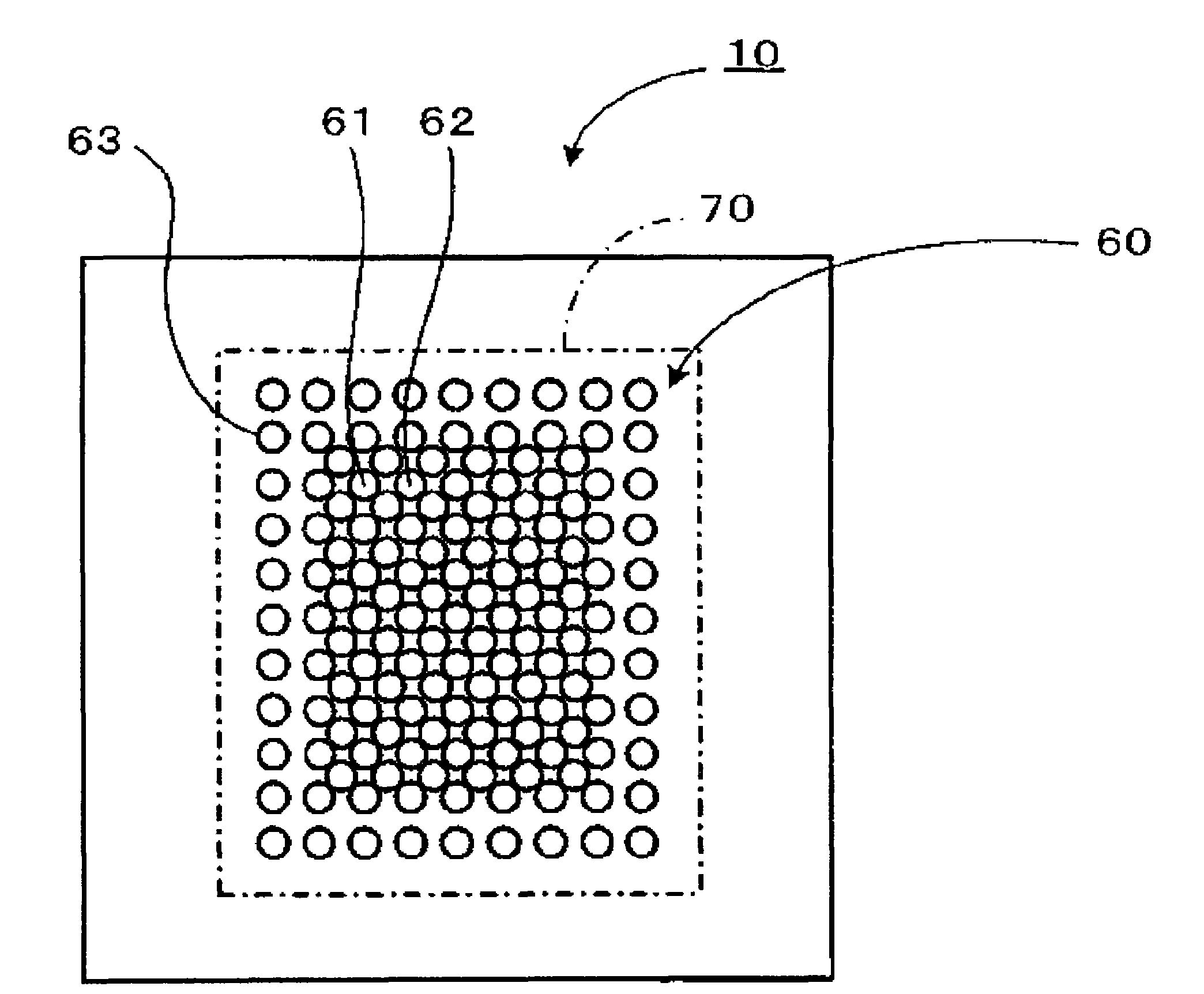
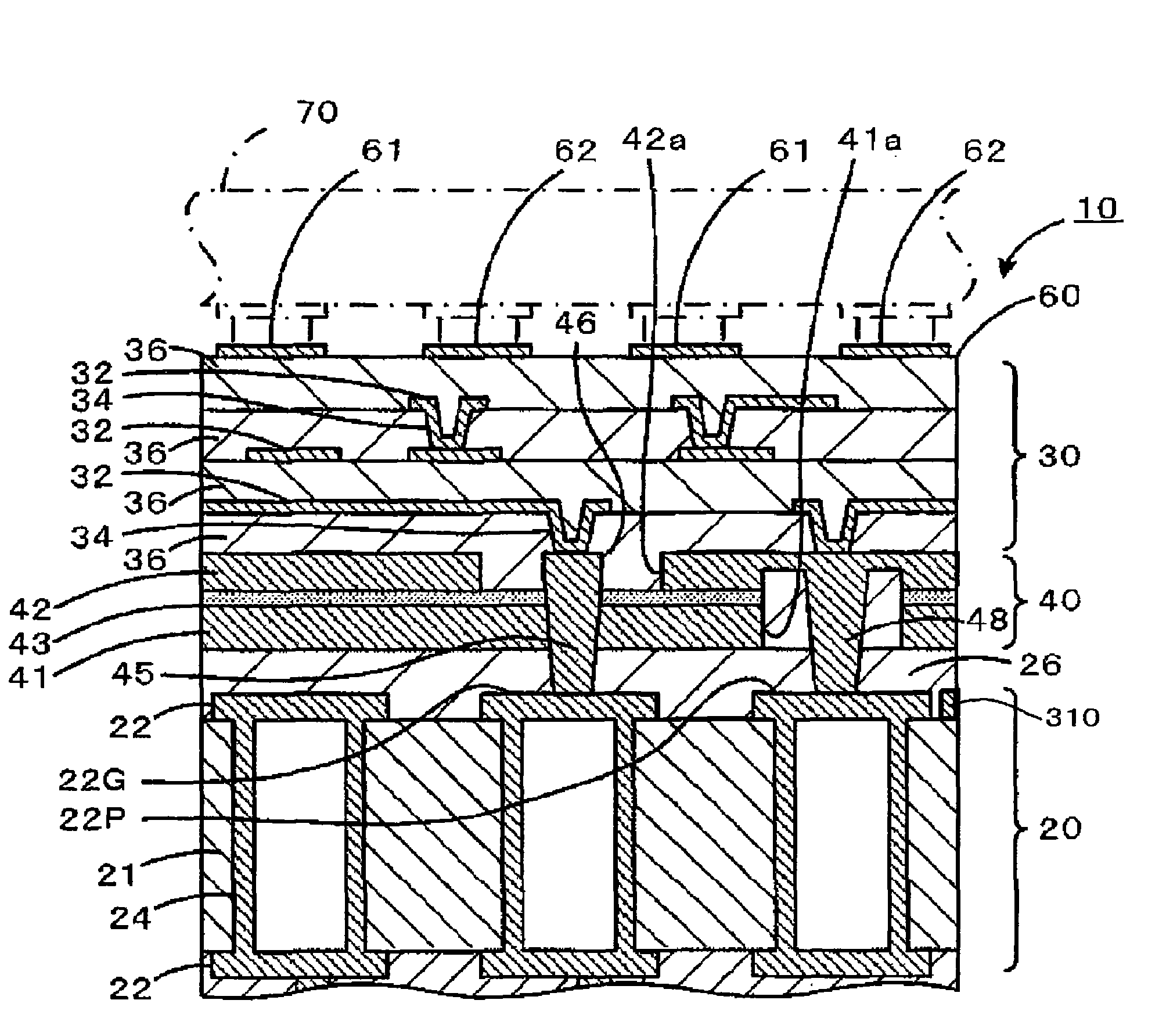
[0044] as a top view figure 1 and as a cross-sectional view of the main part figure 2 The multilayer printed wiring board 10 according to Embodiment 1 is shown. in addition, image 3 A film capacitor 40 inside the multilayer printed wiring board 10 is shown.

[0045] Such as figure 1 As shown, the multilayer printed wiring board 10 of the present embodiment includes a mounting portion 60 on the surface for mounting a semiconductor element 70 . The mounting portion 60 is provided with: a pad 61 connected to a ground line 73 for grounding the semiconductor element 70; a power supply pad 62 connected to a power line 71 for supplying a positive power supply potential to the semiconductor element 70; The signal pad 63 is connected to the signal line 72 for inputting a signal to the semiconductor element 70 or outputting a signal from the semiconductor element 70 (refer to Figure 9 ).

[0046] The pads 61 for grounding and the pads 62 for power supply are arranged in a gri...

Embodiment approach 3

[0111] The manufacturing method of the multilayer printed wiring board 10 which concerns on Embodiment 3 is as follows. First, if Figure 13 As shown in (a), a core substrate 20 is prepared, and a thermosetting insulating film (ABF-45SH manufactured by Ajinomoto Co., Ltd. ) 430 is pasted on the core substrate 20. The thickness of the insulating layer 26 on the core substrate is formed thick, and two thermosetting insulating films 430 are pasted together so that the film capacitor 40 is embedded in the insulating layer 26 on the core substrate. In addition, three or more thermosetting insulating films 430 may be attached.

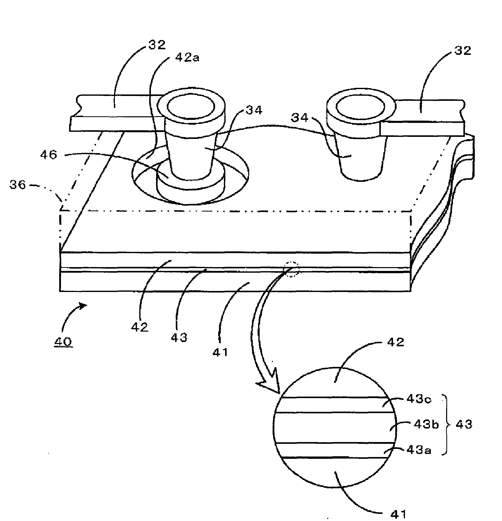
[0112] Next, the high dielectric sheet 420 is positioned and stacked on the thermosetting insulating film 430 in a semi-cured state, wherein the high dielectric sheet 420 uses nickel foil 421 and copper foil 422 to sandwich the high dielectric layer 423 Structure. The alignment mark 310 provided on the core substrate 20 can be used as a mark for position...

other Embodiment approach

[0118] In addition, the present invention is not limited to the above-mentioned embodiments at all, and can be implemented in various forms within the technical scope belonging to the present invention.

[0119] For example, in the above-described embodiment, the ground potential is applied to the ground line 73 and the positive potential is applied to the power line 71 from the power supply PW. Not limited to these at all. A negative potential may be applied from the power supply PW to the ground line 73 , a positive potential may be applied to the power line 71 , or the like. The gist of the invention according to the embodiment is that in a capacitor having electrodes made of different metals, a relatively low potential is applied to the electrode made of a metal with a high ionization tendency, and a relatively low potential is applied to the electrode made of a metal with a low ionization tendency. The formed electrodes apply a relatively high potential.

[0120] In add...


PUM

PropertyMeasurementUnit
thicknessaaaaaaaaaa
thicknessaaaaaaaaaa
thicknessaaaaaaaaaa

Abstract

A multilayer printed wiring board (10) includes a core substrate (20), an on-core-substrate insulating layer (26) laminated on the core substrate (20) and a capacitor section (40) provided on the on-core-substrate insulating layer (26). The capacitor section (40) is formed with a high dielectric layer (43) sandwiched between a lower electrode (41) storing a negative charge and an upper electrode (42) storing a positive charge. An ionization tendency of metal forming the lower electrode (41) is larger than an ionization tendency of metal forming the upper electrode (42). Metal forming the lowerelectrode (41) is nickel and metal forming the upper electrode (42) is copper, for example.

Description

technical field [0001] The invention relates to a multilayer printed circuit board and a manufacturing method thereof. Background technique [0002] A multilayer printed wiring board has been proposed in which wiring patterns laminated in multiple layers via an insulating layer are electrically connected through via holes in the insulating layer. [0003] In such a multilayer printed wiring board, when the mounted semiconductor element is turned on and off at high speed, switching noise may be generated to lower the potential of the power supply line. [0004] Therefore, Patent Document 1 discloses a multilayer printed wiring board capable of decoupling by connecting a capacitor portion between a power supply line and a ground line in order to suppress such a drop in potential. [0005] However, the capacitor portion provided on the multilayer printed wiring board of Patent Document 1 employs a dielectric layer (Dielectric Layer) made of an organic resin mixed with an inorg...

Claims


Application Information

Patent Timeline
Patent Type & Authority Applications(China)
IPC IPC(8): H05K3/46
CPCH05K2201/09309H05K3/4602H05K2201/0352H05K2201/09509H05K1/162H05K2201/09518H05K2201/096H05K2201/09718H05K1/09Y10T29/4913H05K1/18H05K3/46
Inventor 田中宏德清水敬介
Owner IBIDEN CO LTD
Why Eureka
Try Eureka