Supercharge Your Innovation With Domain-Expert AI Agents!

Pixel unit structure of ultraviolet image sensor and preparation method thereof

An image sensor, pixel unit technology, applied in image communication, semiconductor/solid-state device manufacturing, electrical components, etc., can solve problems such as limited sensitivity and resolution, and achieve the effect of improving resolution, simplifying readout circuits, and high sensitivity

Active Publication Date: 2011-01-26
PEKING UNIV
View PDF4 Cites 0 Cited by
  • Summary
  • Abstract
  • Description
  • Claims
  • Application Information

AI Technical Summary

Problems solved by technology

The photoelectric conversion devices of the above-mentioned ultraviolet image sensor pixels are all diode structures, and their sensitivity and resolution are very limited.

Method used


Image

  • Pixel unit structure of ultraviolet image sensor and preparation method thereof
  • Pixel unit structure of ultraviolet image sensor and preparation method thereof
  • Pixel unit structure of ultraviolet image sensor and preparation method thereof

Examples


Embodiment Construction

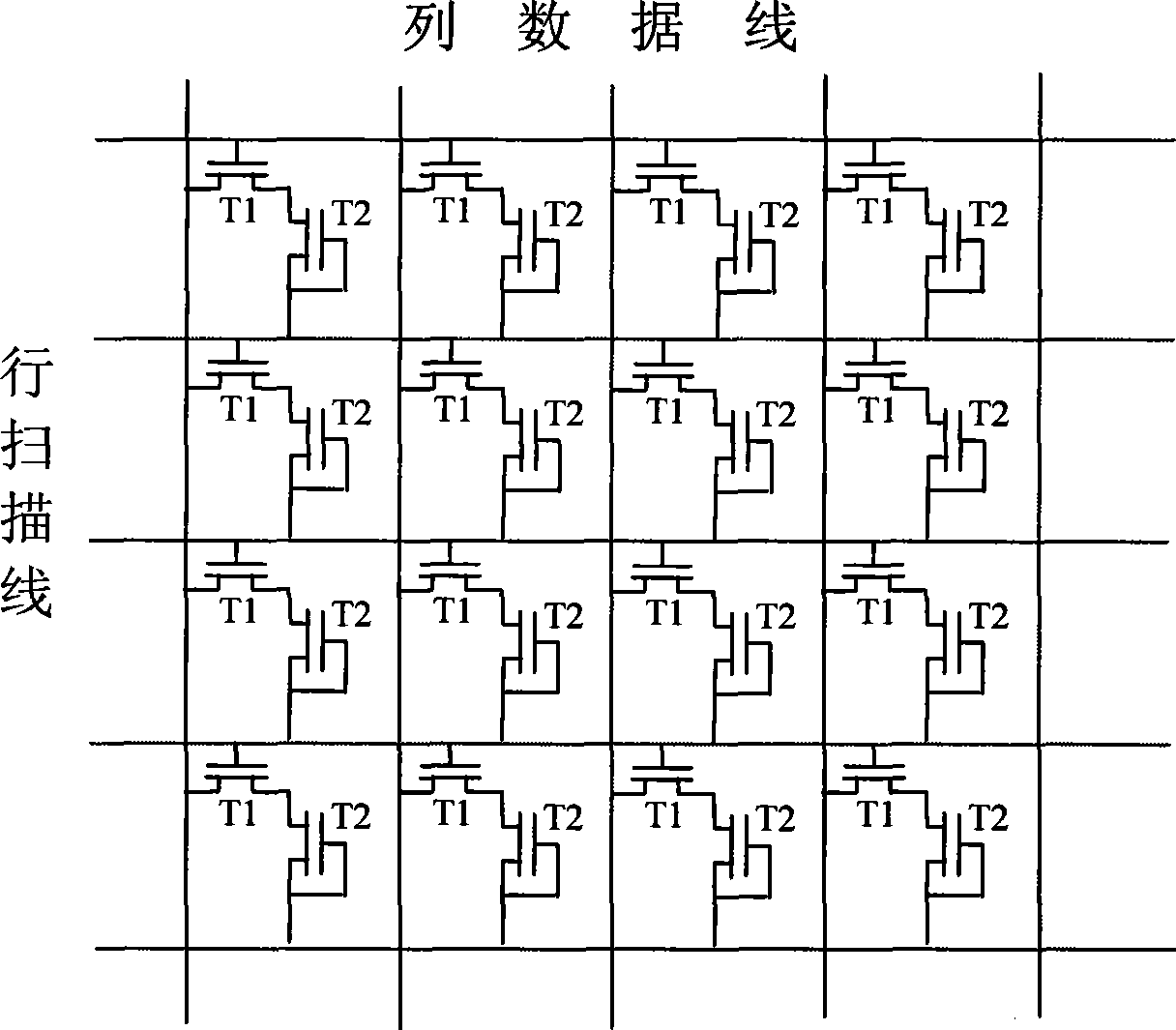
[0045] Adopt the equivalent circuit of the pixel array part of the ultraviolet image sensor of the present invention such as figure 1As shown, it includes a row scan line, a column data line, a drive transistor T1 and an ultraviolet detection transistor T2. The row scanning lines are distributed in parallel, the column data lines are distributed in parallel, the row scanning lines and the column data lines are vertically intersected, and the scanning lines and the data lines are separated by an insulating layer at the intersection. Each rectangular area surrounded by the scan line and the data line is a pixel area. Each pixel is composed of a driving transistor T1 and a detecting transistor T2. The gate electrode of the driving transistor T1 is connected to the corresponding scanning line, and the drain electrode is connected to the corresponding data line. The gate electrode and the source electrode of the detection transistor T2 are connected to the common ground, and the...


PUM


Abstract

The invention discloses a pixel unit of an ultraviolet image sensor and a preparation method thereof. The pixel unit of the sensor comprises a substrate; two thin film transistors are integrated on the substrate, wherein one thin film transistor is a drive transistor comprising a gate electrode, a gate medium, an active layer, a source / drain electrode, a light shielding layer and a passivation layer, while the other thin film transistor is a detection transistor comprising the gate electrode, the gate medium, the active layer, the source / drain electrode and the passivation layer; the gate electrode of the drive transistor is connected with a row scanning line of the image sensor, while the drain electrode of the drive transistor is connected with a column data wire of the image sensor; and the drain electrode of the detection transistor is connected with the source electrode of the drive transistor, while the source electrode of the detection transistor is connected to the ground or connected to the row scanning line of the next row; and the gate electrode of the detection transistor is connected to the ground or biased. Different from a conventional single crystal semiconductor device, the pixel unit of the ultraviolet image sensor has stronger flexibility and lower cost, and considerably improved resolution and sensibility.

Description

technical field [0001] The invention relates to solid-state image sensing technology, in particular to a pixel unit structure of an ultraviolet image sensor and a preparation method thereof. Background technique [0002] Ultraviolet detection technology is widely used in both military and civilian applications. Its applications mainly include disaster alarm under weak daytime light conditions, aerial remote sensing monitoring of organic pollution, high-energy physics research and space detection, satellite ultraviolet communication, military photoelectric countermeasures and infrared / ultraviolet dual-band guidance, etc. High-sensitivity ultraviolet detection generally uses ultraviolet-sensitive photomultiplier tubes and similar vacuum devices, as well as solid-state image sensors represented by ultraviolet-enhanced silicon photodiodes. Compared with solid-state image sensors, vacuum devices have disadvantages such as large volume and high operating voltage; while silicon de...

Claims


Application Information

Patent Timeline
Patent Type & Authority Patents(China)
IPC IPC(8): H01L27/146H01L23/522H01L29/786H01L21/84H01L21/768H04N5/30
Inventor 张盛东王漪金玉丰
Owner PEKING UNIV
Features
  • R&D
  • Intellectual Property
  • Life Sciences
  • Materials
  • Tech Scout
  • Unparalleled Data Quality
  • Higher Quality Content
  • 60% Fewer Hallucinations
Learn More