White light LED packaging structure and packaging method thereof

A technology of LED packaging and LED chips, applied in the direction of electrical components, electrical solid devices, circuits, etc., to achieve the effects of easy process, high conversion efficiency, and small difference in refractive index

Inactive Publication Date: 2010-03-03
SUN YAT SEN UNIV
View PDF0 Cites 23 Cited by
  • Summary
  • Abstract
  • Description
  • Claims
  • Application Information

AI Technical Summary

Problems solved by technology

[0006] Aiming at the problems of heat dissipation, light efficiency, light decay, and light color commonly existing in the packaging of high-power white light LEDs, the present invention provides a packaging structure and packaging method for high-power white light LEDs

Method used


Image

  • White light LED packaging structure and packaging method thereof
  • White light LED packaging structure and packaging method thereof
  • White light LED packaging structure and packaging method thereof

Examples


Embodiment 1

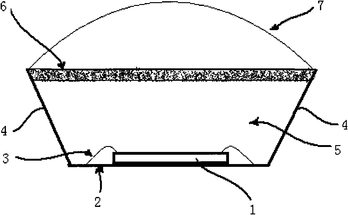
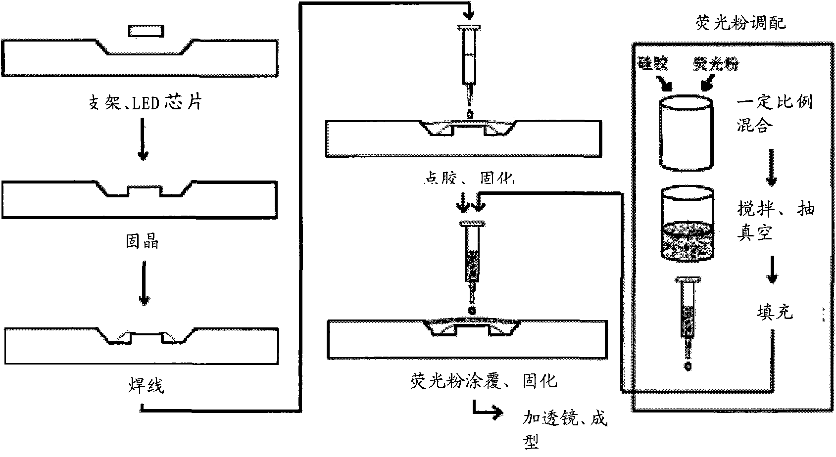
[0034] like figure 1 , figure 2 and image 3As shown in the figure, put a certain amount of silver glue on the cup and bowl of the bracket, put the high-power sapphire substrate GaN blue LED chip 1 on the silver glue of the bracket 2, and perform thermal hardening baking to cure the silver glue. , to fix the LED chip 1 on the bracket 2; weld a gold wire on the electrode of the LED chip 1 to complete the electrical connection with the bracket 2; It is directly coated on the LED chip 1, and after curing, the prepared phosphor is coated on the cured thermal insulation transparent material layer 5 by dispensing or gluing, and cured by baking; Upper peripheral optical components such as lens structures 7 .

Embodiment 2

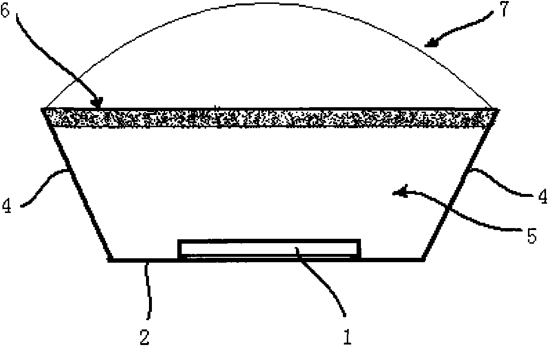
[0036] For the packaged bracket 2 is a plane bracket, such as Figure 4 shown. Then directly coat a certain amount of silica gel on the surface of the LED chip 1 that has been fixed on the bracket 2. Due to the surface tension of the silica gel, it can form an approximate spherical surface. After the silica gel is no longer diffused, put it in the oven and bake at 150°C. After 30 minutes of curing, a heat insulating material layer is formed; the phosphor layer is also coated by the same principle using the same method.

Embodiment 3

[0038] like Figure 5 and Image 6 As shown in the figure, the white LED is encapsulated by the thermal isolation method, and the upper surface of the cured silica gel is coated with two-layer phosphor layers in turn, which are the red phosphor layer 61 and the YAG phosphor layer 62 respectively. Using the coating method of thermally isolated double-layer phosphor layer, the obtained white light LED has a higher color rendering index (Ra can reach more than 90), better light color stability and better heat dissipation effect than the existing white light LED. .


PUM


Abstract

The invention discloses a white light LED packaging structure comprising a bracket and a plurality of LED chips arranged on the bracket, wherein a heat-insulation transparent material layer is coatedon the LED chips, a fluorescent powder layer is also coated on the heat-insulation transparent material layer, and a light outlet face of the heat-insulation transparent material layer and the fluorescent powder layer directly form a lens structure, or a lens structure is arranged on the fluorescent powder layer. The number of the LED chip is multiple, the heat-insulation transparent material layer and the fluorescent powder layer are sequentially and independently coated on each LED chip, or the heat-insulation transparent material layer and the fluorescent powder layer are integrally coatedon each LED chip. The invention has low manufacturing cost, improves the problem of heat radiation of a high-power white light LED, reduces light attenuation and enables the light color to be more stable.

Description

technical field [0001] The invention relates to the technical field of LED packaging, in particular to a white light LED packaging structure and a packaging method thereof. Background technique [0002] LED is a semiconductor light-emitting device, which can directly convert electrical energy into visible light and radiant energy. It has a series of characteristics such as low operating voltage, low power consumption, high luminous efficiency, light weight and small size, so it is widely used Used in indicator lights, display screens, etc. With the rapid development of high-power LEDs, white LEDs have gradually entered the field of general lighting and are known as the fourth generation of lighting sources. In addition to the RGB combination to form a white light LED, there is also a blue or ultraviolet light chip to excite the phosphor. The light emitted by the chip under the action of electricity partially excites the phosphor to generate a longer wavelength band of visib...

Claims


Application Information

Patent Timeline
Patent Type & Authority Applications(China)
IPC IPC(8): H01L33/00H01L25/075H01L23/28H01L23/13H01L23/31H01L23/373H01L21/50H01L21/56
Inventor 张佰君蚁泽纯
Owner SUN YAT SEN UNIV
Why Eureka
Try Eureka