Bias circuit used in Ku waveband internally-matched field effect transistor

A field effect transistor and bias circuit technology, applied in the direction of amplifiers with distributed constants in the coupling network, etc., can solve the problems of poor broadband performance and large insertion loss, and achieve the effects of small insertion loss, widening bandwidth and eliminating low-frequency oscillation.

Active Publication Date: 2010-03-03
INST OF MICROELECTRONICS CHINESE ACAD OF SCI
View PDF0 Cites 19 Cited by
  • Summary
  • Abstract
  • Description
  • Claims
  • Application Information

AI Technical Summary

Problems solved by technology

[0006] However, the broadband performance of this structure is poor, and it will introdu

Method used


Image

  • Bias circuit used in Ku waveband internally-matched field effect transistor
  • Bias circuit used in Ku waveband internally-matched field effect transistor
  • Bias circuit used in Ku waveband internally-matched field effect transistor

Examples


Embodiment Construction

[0033] In order to make the object, technical solution and advantages of the present invention clearer, the present invention will be described in further detail below in conjunction with specific embodiments and with reference to the accompanying drawings.

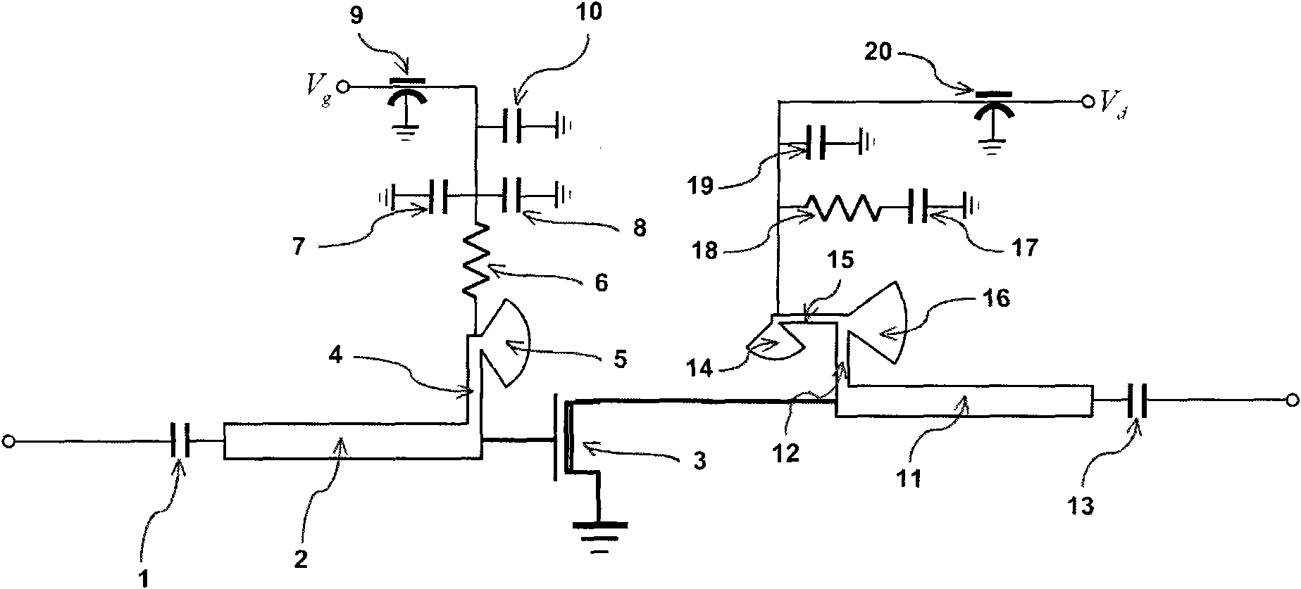
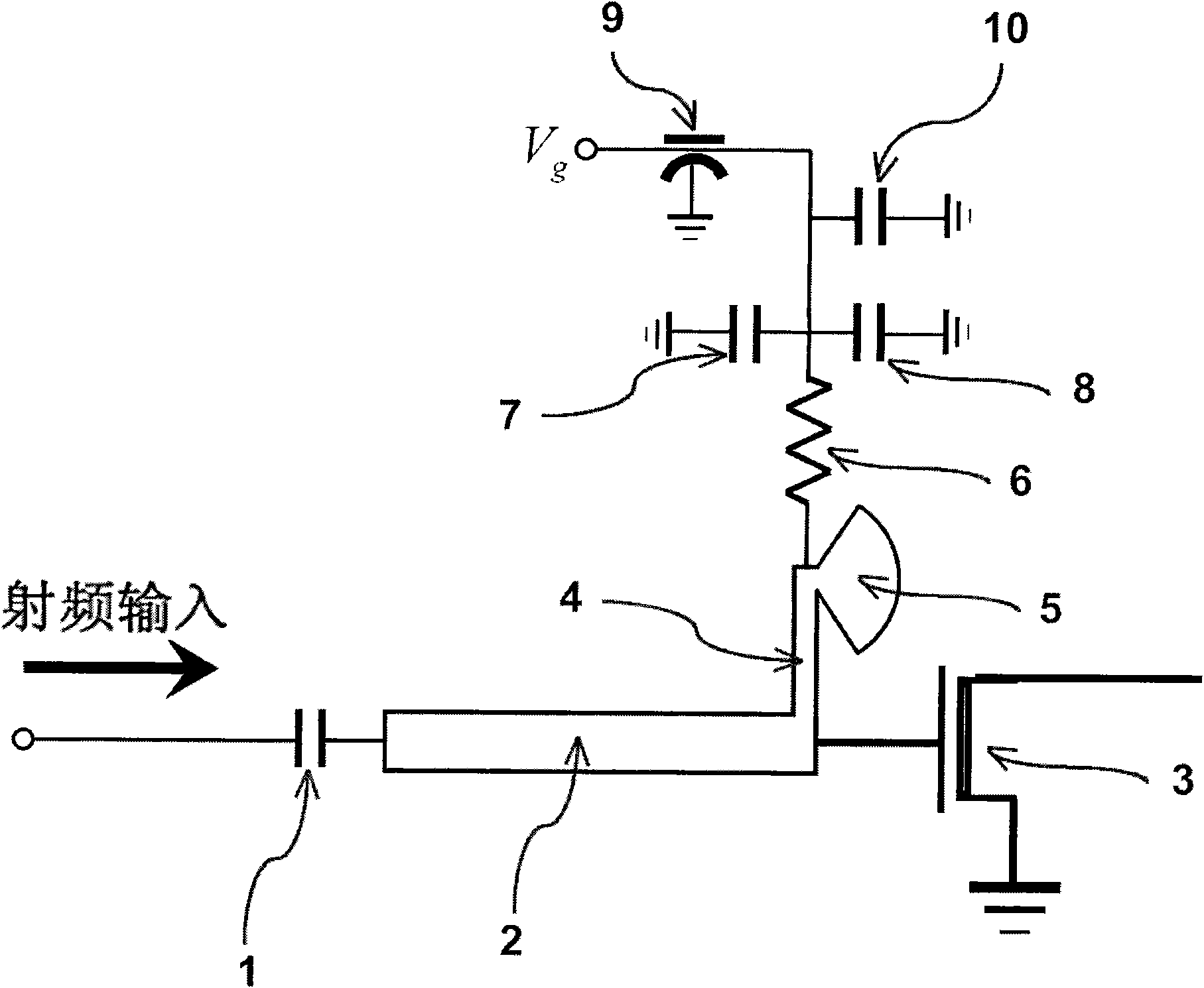
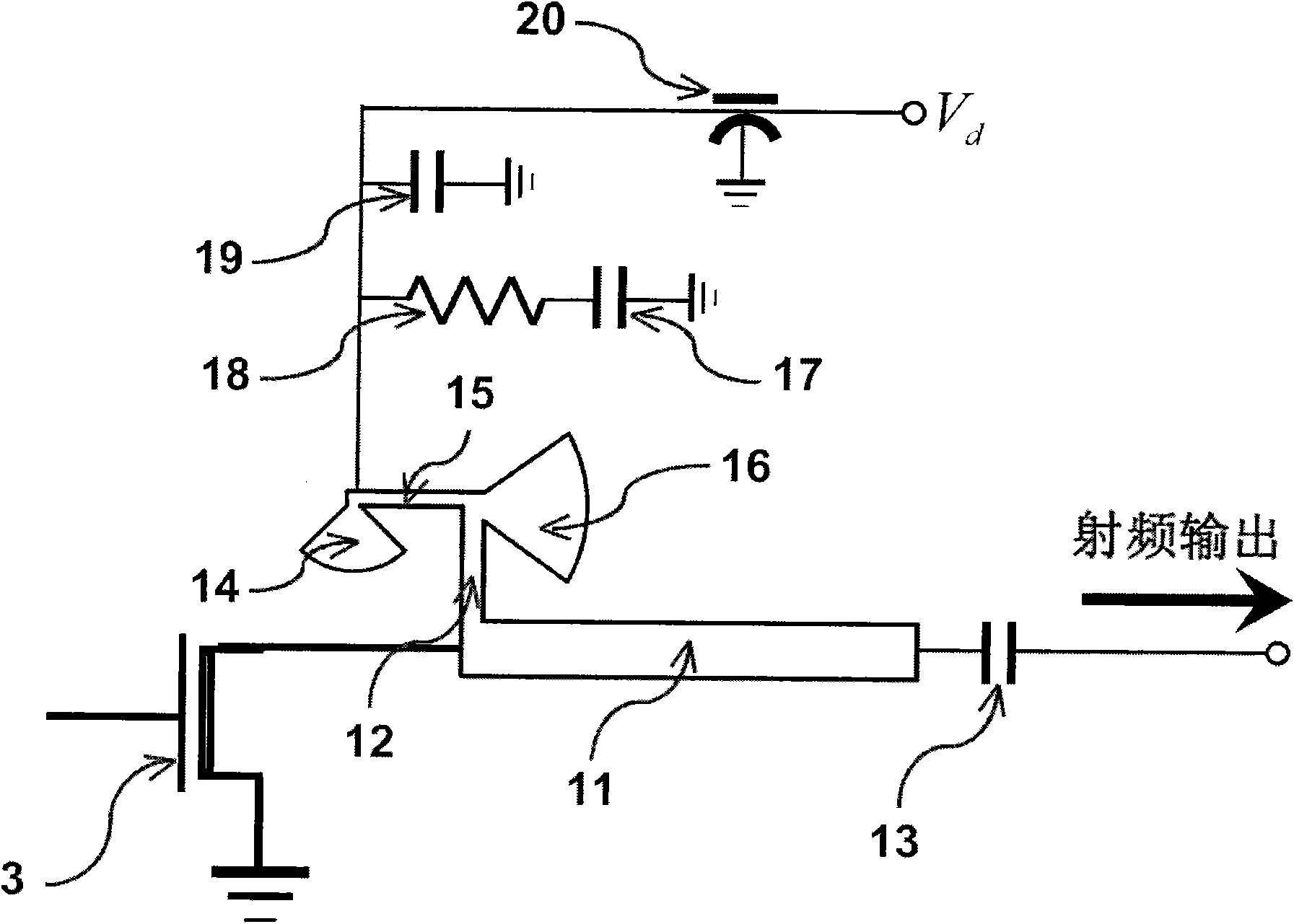
[0034] The present invention can be applied to any microwave power amplifier based on matching field-effect transistors in the Ku band, now combined figure 1 , figure 2 and image 3 The present invention is described in detail:

[0035] Such as figure 1 as shown, figure 1 It is a schematic diagram of a bias circuit for matching field effect transistors in the Ku band provided by the present invention. The bias circuit consists of a gate bias circuit with a microstrip stub structure, a matching field effect transistor in the Ku band, and a double-segment microstrip Drain bias circuit with stub structure. Wherein, the gate bias circuit of the microstrip stub structure is connected to the gate of the matching field eff...


PUM


Abstract

The invention discloses a bias circuit used in a Ku waveband internally-matched field effect transistor. The bias circuit is characterized in that the bias circuit consists of a grid bias circuit of amicrostrip stub structure, the Ku waveband internally-matched field effect transistor and a drain bias circuit of a dual-segment microstrip stub structure, wherein the grid bias circuit is connectedwith the grid of the Ku waveband internally-matched field effect transistor, while the drain bias circuit is connected with the drain of the Ku waveband internally-matched field effect transistor. Thebias circuit can effectively restrain low-frequency oscillation which frequently occurs inside a Ku waveband microwave power amplifier, thereby increasing the stability of the amplifier and broadening the bandwidth of the bias circuit at very low insertion loss. Therefore, the bias circuit can be used in various Ku waveband microwave power amplifiers based on internally-matched field effect transistors.

Description

technical field [0001] The invention relates to the technical field of microwave power amplifiers, in particular to a bias circuit for matching field effect transistors in the Ku band. Background technique [0002] In radar transmitter systems, electronic countermeasures, intelligent missiles, and various communication and navigation electronic systems, microwave power amplifiers using Ku-band matched field-effect transistors as active devices are widely used. [0003] Since the DC power supply and microwave signal input and output of most internally matched field effect transistors share pins, the bias circuit and the microwave link will interact with each other, which may cause low-frequency oscillation of the microwave power amplifier, microwave signal leakage through the bias circuit, and power loss. Amplifier gain and phase variations create distortion. [0004] For the internally matched microwave power tubes in the lower frequency band, the DC bias is generally provi...

Claims


Application Information

Patent Timeline
IPC IPC(8): H03F3/60
Inventor 陈高鹏陈晓娟刘新宇李滨
Owner INST OF MICROELECTRONICS CHINESE ACAD OF SCI
Why Eureka
Try Eureka