Circuit board, display device and liquid crystal display device
A circuit substrate and circuit technology, applied in identification devices, printed circuit components, optics, etc., can solve problems such as aluminum film corrosion
- Summary
- Abstract
- Description
- Claims
- Application Information
AI Technical Summary
Problems solved by technology
Method used
Image
Examples
Embodiment approach 1
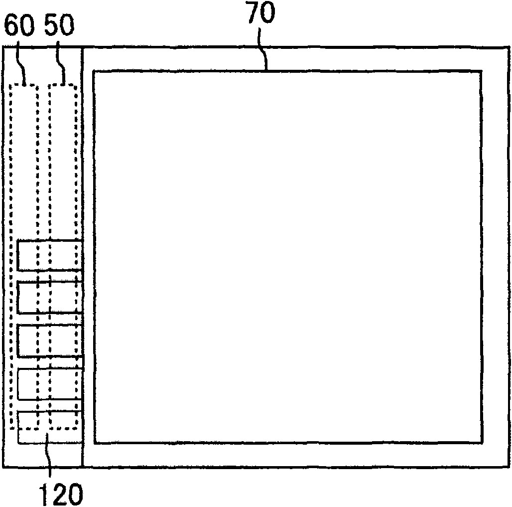
[0131] Picture 1-1 It is a plan schematic view showing the structure of the circuit board according to Embodiment 1.
[0132] Such as Picture 1-1 As shown, the external connection terminal 120 has a form in which the circuit region 50 and the peripheral wiring region 60 are provided in a layer below the external connection terminal 120 , so that the area of the display region 70 can be increased. The "circuit area" is an area where circuit structural wires constituting the circuit are densely arranged, and the "peripheral wiring area" is an area where peripheral wires that transmit signals from external connection terminals to the drive circuit are densely arranged.
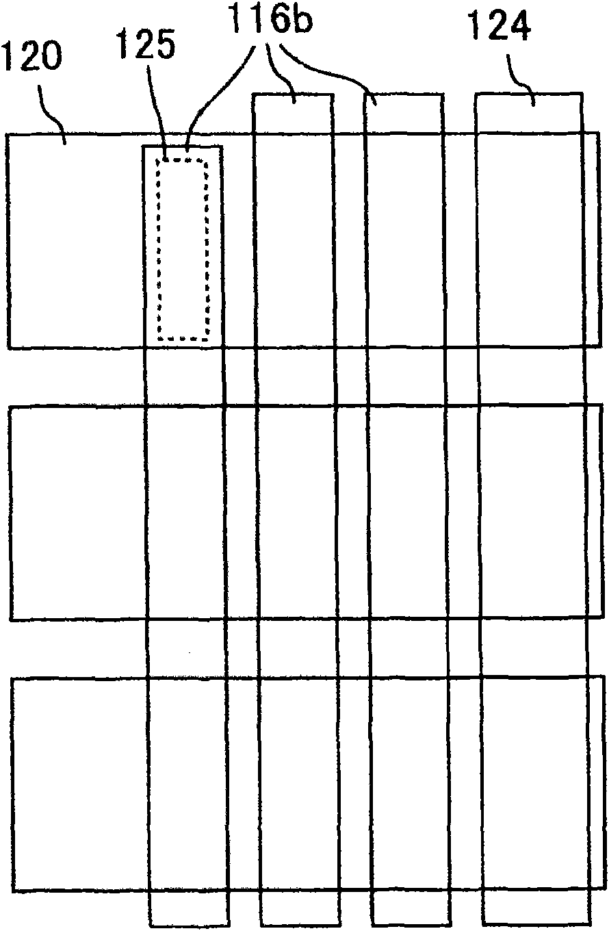
[0133] A pixel electrode composed of a reflective electrode and a transparent electrode is arranged in the display region 70 . also, Figure 1-2 In the circuit board according to Embodiment 1, it represents Picture 1-1 An enlarged schematic plan view of the arrangement relationship between the peripheral...
Embodiment approach 2
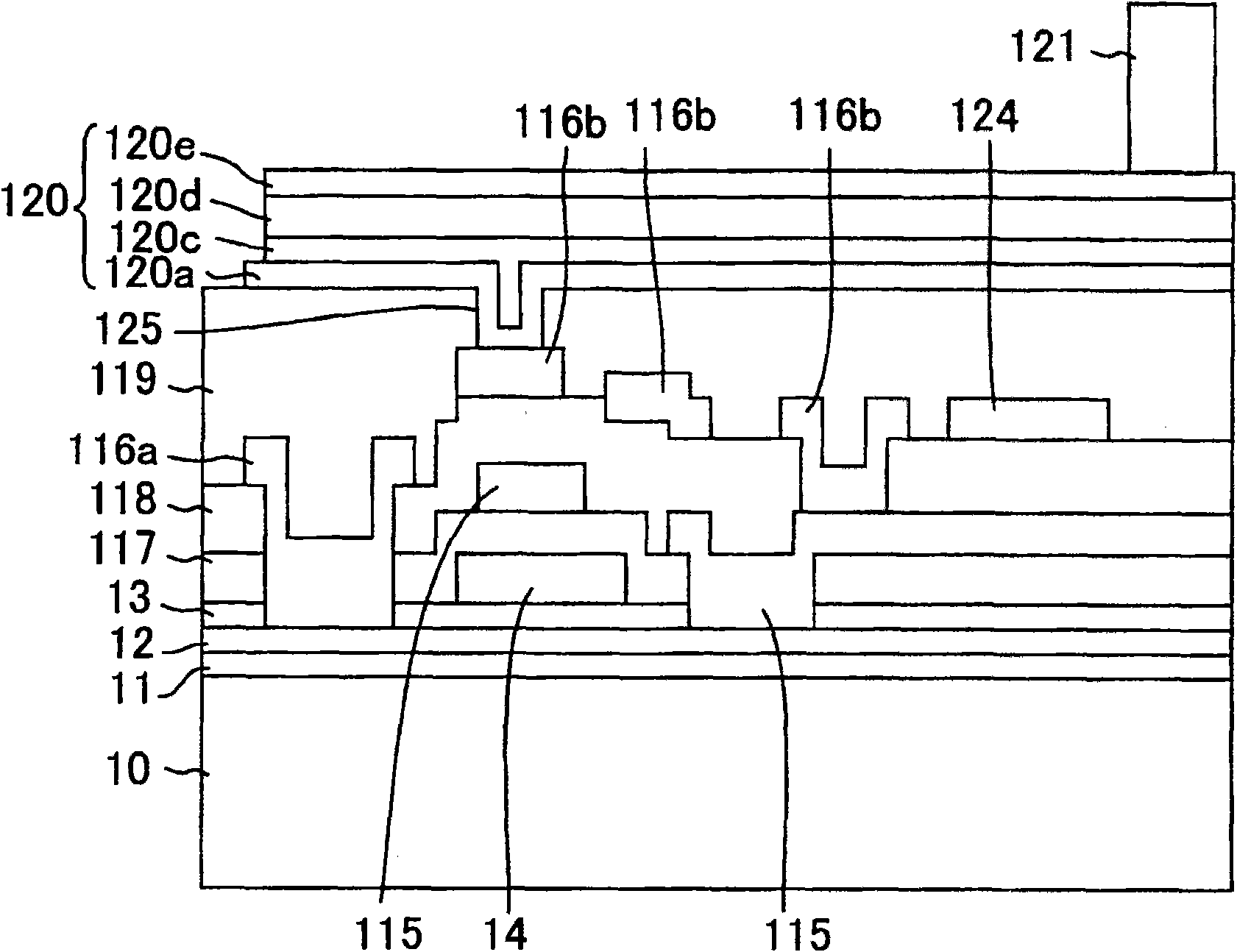
[0176] figure 2 It is a schematic cross-sectional view showing the structure around the external connection terminals of the circuit board according to the second embodiment.
[0177] In the circuit board according to the second embodiment, the structure of the layer below the gate electrode is the same as that of the first embodiment, such as figure 2 As shown, an undercoat film 11 , a semiconductor layer 12 , a gate insulating film 13 , and a gate electrode 14 formed on a substrate 10 are arranged. A first interlayer insulating film 217 and a second interlayer insulating film 218 are disposed on the gate electrode 14 . Source / drain electrodes 215 are arranged on the second interlayer insulating film 218 . The source / drain electrodes 215 are connected to the semiconductor layer 12 through contact holes formed in the gate insulating film 13 , the first interlayer insulating film 217 , and the second interlayer insulating film 218 .
[0178] A third interlayer insulating fil...
Embodiment approach 3
[0180] image 3 It is a cross-sectional schematic view showing the structure around the external connection terminals of the circuit board according to Embodiment 3.
[0181] The circuit board according to Embodiment 3 is the same as Embodiment 2 with respect to the structure of layers below the gate / drain electrodes 315 . Such as image 3 As shown, an undercoat film 11, a semiconductor layer 12, a gate insulating film 13, a gate electrode 14, a first interlayer insulating film 317, a second interlayer insulating film 318, and a source electrode formed on a substrate 10 are sequentially arranged. / drain electrode 315 . A third interlayer insulating film 319 made of silicon nitride is formed on the source / drain electrodes 315 , and a peripheral wiring 316 b and a power supply wiring 324 are provided on the third interlayer insulating film 319 . The fourth interlayer insulating film 323 and the external connection terminal 320 are sequentially provided on the peripheral wirin...
PUM
 Abstract
Description
Claims
Application Information
 - R&D
- Intellectual Property
- Life Sciences
- Materials
- Tech Scout
- Unparalleled Data Quality
- Higher Quality Content
- 60% Fewer Hallucinations
Browse by: Latest US Patents, China's latest patents, Technical Efficacy Thesaurus, Application Domain, Technology Topic, Popular Technical Reports.
© 2025 PatSnap. All rights reserved.Legal|Privacy policy|Modern Slavery Act Transparency Statement|Sitemap|About US| Contact US: help@patsnap.com


