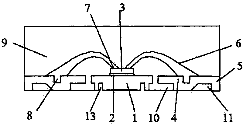
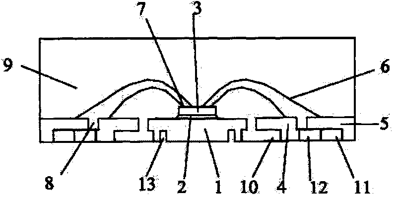
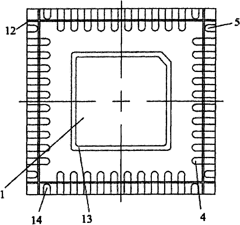
Packaging part with double-row pins and four flat and pin-free surfaces and production method thereof
A leadless packaging, four-sided flat technology, applied in the direction of electrical components, electrical solid state devices, semiconductor devices, etc., can solve the problems of unsatisfactory product packaging, less pins, and restrictions on the expansion of packaging technology
- Summary
- Abstract
- Description
- Claims
- Application Information
AI Technical Summary
Problems solved by technology
Method used
Image
Examples
Embodiment 1
[0043] 1. Thinning and scribing
[0044] Thinning thickness is 50μm, stack package, roughness Ra 0.10mm.
[0045] 8″ wafer thickness thinning: DR3000III / NITIO for placement machine,
[0046] 8″ thinning machine: PG300RM / TSN. Thickness gauge DH151 / TSK;
[0047] 8″ dicing machine: use a double-knife dicing machine, using anti-separation layer and anti-fragmentation process for scribing.
[0048] 2. Core loading
[0049] 8″ uses AD829 core loading machine;
[0050] Adhesive film is used as the adhesive material, and the lead frame is a four-sided flat leadless frame with double rows of pins. ESPEC oven is used, and the nitrogen flow rate is 25-35L / min.
[0051] 3. Pressure welding
[0052] ESEC3100 and Eagle60 bonding machines are selected, and the welding wire material is gold wire. Since the thickness of the package is 0.75, the pressure welding adopts the ultra-low-line arc pressure welding process, and the high-low arc positive and negative bonding method avoids the phen...
Embodiment 2
[0064] 1. Thinning and scribing
[0065] Thinning thickness 200μm stacked package, roughness Ra 0.05mm,
[0066] 12″wafer thickness reduction: DR3000III / NITI0 for placement machine,
[0067] 12″ thinning machine: PG300RM / TSN. Thickness gauge DH151 / TSK,
[0068] 12″ dicing machine: WD300TXB, DR3000III / TSK for SMT,
[0069] Anti-separation layer, anti-shards process scribing.
[0070] 2. Core loading
[0071] 12″ choose DB-700FC / Jupei chip bonder.
[0072] Adhesive film material: Adhesive film or insulating glue is used, the lead frame is a four-sided flat leadless frame with double rows of pins, an ESPEC oven is used, and the nitrogen flow rate is (25-35) L / min.
[0073] 3. Pressure welding
[0074] Eagle60 bonding machine is used for pressure welding, copper wire is used for welding wire material, ultra-low arc pressure welding process is adopted for pressure welding, and high and low arc positive and negative welding methods are used to avoid wire crossing and broken wi...
Embodiment 3
[0086] 1. Thinning and scribing
[0087] According to the thickness of the packaged product, the thinning thickness is determined to be 150μm, and the roughness Ra is 0.08mm.
[0088] Mounter with DR3000III / NITI0,
[0089] 6″wafer use: VG502MKII 8B.
[0090] Thinning machine: PG300RM / TSN. Thickness gauge DH151 / TSK;
[0091] 6″ slice dicing machine: DAD3350.
[0092] The scribing tool is selected according to the width of the scribing lane of the product, and the anti-separation layer and anti-fragmentation process are adopted.
[0093] 2. Core loading
[0094] Use AD89 core loading machine;
[0095] Bonding material: 8200 series materials are selected, and the lead frame is a four-sided flat lead-free frame with double rows of pins. The application adopts an ESPEC oven, and the nitrogen flow rate is (25-35) L / min.
[0096] 3. Pressure welding
[0097] Eagle60 bonding machine is used for pressure welding, and gold wire is used as the welding wire material. Since the pack...
PUM
| Property | Measurement | Unit |
|---|---|---|
| Thickness | aaaaa | aaaaa |
| Thickness | aaaaa | aaaaa |
| Coefficient of expansion | aaaaa | aaaaa |
Abstract
Description
Claims
Application Information


