Two-dimensional wavelet transformation integrated circuit structure

An integrated circuit, two-dimensional wavelet technology, applied in logic circuits, televisions, electrical components, etc., can solve problems such as high computational complexity, long system output delay, and less output delay, and achieve the effect of reducing hardware resources.

Inactive Publication Date: 2010-04-21
HUAZHONG UNIV OF SCI & TECH
View PDF0 Cites 13 Cited by
  • Summary
  • Abstract
  • Description
  • Claims
  • Application Information

AI Technical Summary

Problems solved by technology

The advantage of this structure is that the control is simple, but the biggest disadvantage is that a large-scale intermediate data buffer memory is required. In addition, it also has high computational complexity and long system output delay.
See Xiong[5] for direct structure based on line sweep: Cheng-Yi Xiong, Jin-Wen Tian, ​​JianLiu, "Efficient High-Speed/Low-Power Line-Based Architecture

Method used


Image

  • Two-dimensional wavelet transformation integrated circuit structure
  • Two-dimensional wavelet transformation integrated circuit structure
  • Two-dimensional wavelet transformation integrated circuit structure

Examples


Embodiment Construction

[0022] The present invention will be described in detail below in conjunction with the accompanying drawings and implementation examples.

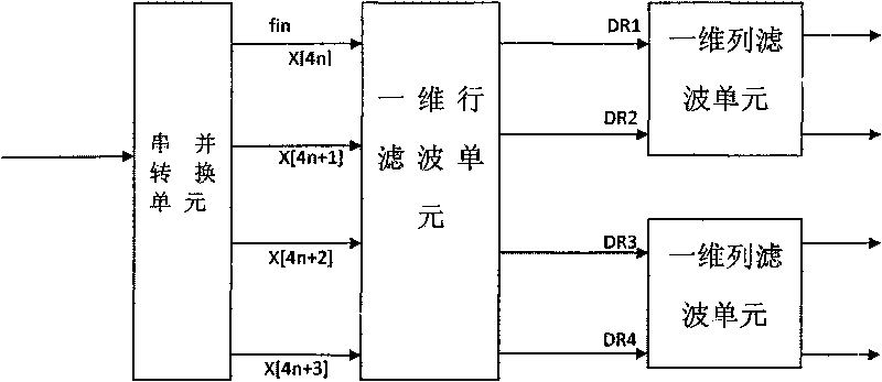
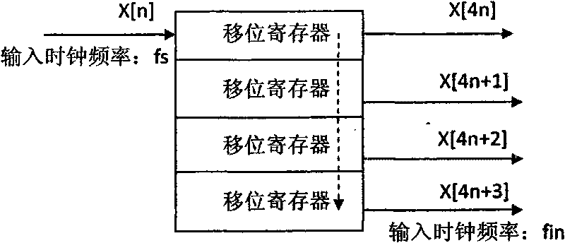
[0023] figure 1It is a structural block diagram of the present invention, including a serial-to-parallel conversion circuit, a one-dimensional row filter circuit and a one-dimensional column filter circuit; in many applications, data is sent to the system row by row from left to right in a serial manner for processing. In order to process the input image data in parallel, we first send it to the serial-to-parallel conversion circuit, so that four adjacent data in the same row have parallelism. Therefore, the output frequency (internal clock frequency) of the serial-to-parallel conversion circuit is 1 / 4 of the input frequency. The one-dimensional row filter circuit processes four input data at the same time, and can complete the one-dimensional row wavelet transform within a unit internal clock cycle, and output four row-transformed wavele...


PUM


Abstract

The invention provides a two-dimensional wavelet transformation integrated circuit structure, belongs to the fields of wavelet transformation in a super-large-scale integrated circuit design technique and an image processing technique and an image compression processing technique, and aims to improve the response speed and the output speed of the whole conversion circuit structure. The two-dimensional wavelet transformation integrated circuit structure comprises a serial-parallel conversion circuit, a one-dimensional line filter circuit and one-dimensional row filter circuits, wherein the serial-parallel conversion circuit is used for converting inputted image data into parallel data and sending the parallel data to the one-dimensional line filter circuit; in a unit internal clock cycle, the one-dimensional line filter circuit outputs four line filter coefficients to two one-dimensional row filter circuits; and the two one-dimensional row filter circuits finish the whole row filter operation and output a result. Compared with the conventional method, the two-dimensional wavelet transformation integrated circuit structure has the characteristics of shorter operational time, less internal memories and shorter output time delay, quicker system response, higher output speed and the like, and is suitable in fields where the high-speed operation is needed and the like.

Description

technical field [0001] The invention belongs to the wavelet transform field in VLSI design technology, image processing, and image compression processing technology, and specifically relates to a two-dimensional wavelet transform integrated circuit structure. Background technique [0002] The most successful application field of wavelet transform is image compression. The theory and algorithm of wavelet transform clearly put forward some enlightening ideas. A key idea is multi-resolution decomposition, which is well used in the research of wavelet image coding. The research on wavelet image compression shows that many features required by modern applications, such as multi-resolution, multi-layer quality control, embedded code stream, etc., are naturally integrated with wavelet image coding structure. Under a large compression ratio, wavelet image Compressed reconstruction quality is also significantly better than DCT transform method. The traditional convolution-based wav...

Claims


Application Information

Patent Timeline
IPC IPC(8): H03K19/00G06F17/14G06T9/00H04N7/26
Inventor 田昕田金文谭毅华
Owner HUAZHONG UNIV OF SCI & TECH
Why Eureka
Try Eureka