

Intermediate infrared antimonide laser device structure adopting DWELL
A technology of antimonides and lasers, which is applied to lasers, laser components, semiconductor lasers, etc., can solve problems such as difficulty, affecting device performance, and low efficiency of a single quantum dot layer, so as to improve efficiency, improve overall performance, and improve electro-optic The effect of conversion efficiency
- Summary
- Abstract
- Description
- Claims
- Application Information
AI Technical Summary
Problems solved by technology
Method used
Image

Examples
Embodiment Construction
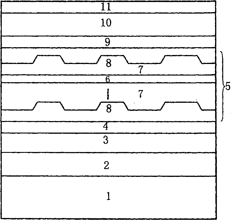
[0009] like figure 1 As shown, a mid-infrared antimonide laser structure using DWELL includes: n-type GaSb substrate (1), n-type GaSb buffer layer (2), n-type Al 0.9 Ga 0.1 As 0.03 Sb 0.97 Lower confinement layer (3), n-type Al 0.3 Ga 0.7 As 0.02 Sb 0.98 Lower waveguide layer (4), DWELL layer (5), DWELL layer (5) including barrier layer Al 0.3 Ga 0.7 As 0.02 Sb 0.98 (6), quantum well layer In 0.2 Ga 0.8 As 0.02 Sb 0.98 (7), InGaSb quantum dot layer (8), p-type Al 0.3 Ga 0.7 As 0.02 Sb 0.98 Upper waveguide layer (9), p-type Al 0.9 Ga 0.1 As 0.03 Sb 0.97 An upper confinement layer (10), a p+ type GaSb ohmic layer (11). The substrate (1) is the substrate for material epitaxial growth, using a Te-doped GaSb substrate; a 0.5 μm Te-doped GaSb buffer layer (2) is grown; the lower confinement layer is Al with a thickness of 1.2 μm and an Al content of 0.9 0.9 Ga 0.1 As 0.03 Sb 0.97 Layer (3); the lower waveguide layer is Al with a thickness of 0.35 μm and an ...
PUM
| Property | Measurement | Unit |
|---|---|---|
| Thickness | aaaaa | aaaaa |
| Thickness | aaaaa | aaaaa |
| Thickness | aaaaa | aaaaa |
Abstract
Description
Claims
Application Information