LED light source using PMMA optical filter
An LED light source and optical filter technology, applied in the field of optical filtering, can solve the problems of no band filtering, no filtering, etc., and achieve the effects of high ultraviolet cutoff rate, simple preparation method, and reducing the harm of light radiation.
- Summary
- Abstract
- Description
- Claims
- Application Information
AI Technical Summary
Problems solved by technology
Method used
Image
Examples
Embodiment 1
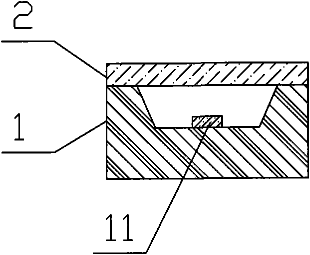
[0043] see figure 1 , an LED device 1, in which an LED chip 11 is packaged, and a PMMA filter 2 is located above the LED chip 11 and fixed.
[0044] When working, the light emitted by the LED chip 11 must pass through the optical filter 2 before it can be emitted to the outside. The optical filter 2 filters the light emitted by the LED chip within the range of wavelengths less than 445nm and greater than 700nm.
[0045] LED chip 11 can choose any desired emission wavelength, such as green light with a dominant wavelength of 530nm, or red light with a dominant wavelength of 620nm; another example is blue light with a dominant wavelength of 460nm, and mix a certain proportion in the potting glue YAG powder, the blue light emitted by the LED chip excites the YAG powder, and finally obtains white light with a color temperature of 8000K or other required color temperatures.
[0046] The preparation of the optical filter with dual functions of cutting off ultraviolet rays and infra...
Embodiment 2
[0058] It is basically the same as that of Example 1, except that the preparation of the optical filter is carried out by magnetron sputtering coating inner layer film on PMMA transparent substrate by silicon target material and tantalum pentoxide target material first, on this basis, then by The titanium oxide-cerium oxide target is subjected to magnetron sputtering to coat the outer film to obtain the product.
Embodiment 3
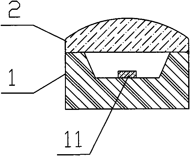
[0060] Basically the same as Embodiment 1, the difference is that the optical filter is molded into a circular lens surface by a PMMA transparent substrate, such as figure 2 shown; or shaped into a square lens surface, and then cleaned and coated.
PUM
 Abstract
Description
Claims
Application Information


