Nano chemical sensor based on semiconductor nanowire and capable of supplying power by self and preparation method thereof

A chemical sensor and semiconductor technology, which is applied in the field of nano chemical sensor and preparation, and can solve problems such as integration and application limitations

Inactive Publication Date: 2010-05-19
UNIV OF SHANGHAI FOR SCI & TECH
View PDF0 Cites 11 Cited by
  • Summary
  • Abstract
  • Description
  • Claims
  • Application Information

AI Technical Summary

Problems solved by technology

However, this kind of semiconductor nanochemical sensor needs an external power supply in the working process. Due to the large scale of the power supply itself and the limitation of life, the integration and application of such devices are limited to a certain extent.

Method used


Image

  • Nano chemical sensor based on semiconductor nanowire and capable of supplying power by self and preparation method thereof
  • Nano chemical sensor based on semiconductor nanowire and capable of supplying power by self and preparation method thereof
  • Nano chemical sensor based on semiconductor nanowire and capable of supplying power by self and preparation method thereof

Examples


Embodiment 1

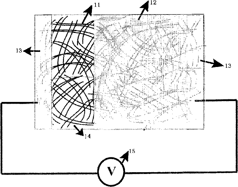
[0022] see figure 1 , the self-powered nanochemical sensor based on semiconductor nanowires of the present invention includes: substrate ( figure 1 Not shown in ), semiconductor nanowire 11 , sealing layer 12 , and two electrodes 13 .

[0023] The substrate is non-conductive and non-reactive with organic chemical molecules. In this embodiment, the substrate is composed of a silicon single crystal covered with an oxide layer of about 300 nm.

[0024] The semiconductor nanowires 11 are grown on the surface of the substrate, and there are a plurality of them, which are randomly arranged and intertwined to conduct with each other. In this embodiment, the semiconductor nanowires 11 are p-type nanowires formed of silicon, with an average diameter of 30 nm and a length of about 10 um. In addition, n-type or p-type nanowires formed of zinc oxide, germanium, or gallium nitride may also be used.

[0025] The material of the sealing layer 12 is non-conductive, insoluble in organic c...

Embodiment 2

[0036] See Figure 4 , the self-powered nanochemical sensor based on semiconductor nanowires in this embodiment includes: a substrate 20 , a semiconductor nanowire 21 , a sealing layer 22 , and two electrodes 23 . Among them, a plurality of semiconductor nanowires 21 are n-type zinc oxide nanowires, arranged vertically and orderly along the substrate direction, and their bottoms are connected to each other, and the part covered by the sealing layer 22 is more than the part not covered by the sealing layer 22, each The diameter is about 20-200nm, the length is about 6-10um, and the length of the exposed part is about 1um. The sealing layer 22 is a PVC polymer. The two electrodes 23 are Au / Ti thin films, the electrode at the top is in contact with the exposed zinc oxide nanowires, and the other metal electrode is formed by conductive silver glue, which is in contact with the zinc oxide thin film layer on the surface of the substrate so that multiple semiconductor nanowires are ...


PUM

PropertyMeasurementUnit
diameteraaaaaaaaaa

Abstract

The invention relates to a nano chemical sensor based on a semiconductor nanowire and capable of supplying power by self and a preparation method thereof. The nano chemical sensor comprises a semiconductor nanowire, wherein the semiconductor nanowire grows on a substrate which is non-conductingg and can not react with an organic chemical molecule; one part of the growing semiconductor nanowire is covered by a seal layer which is non-conductive, not dissolved in an organic chemical solvent and water and does not react with the semiconductor nanowire and electrodes; one of the electrodes is connected with the semiconductor nanowire sealed by the seal layer, and the other electrode is connected with the semiconductor nanowire which is not sealed by the seal layer; when the nano chemical sensor is in contact with a chemical substance, a potential difference can be generated between the part covered by the seal layer and the part which is not sealed, thereby carrying out quantitative and qualitative detection without adding a power supply.

Description

technical field [0001] The invention relates to a nanometer chemical sensor and a preparation method, in particular to a nanometer chemical sensor based on semiconductor nanowires and capable of self-power supply and a preparation method. Background technique [0002] In recent years, chemical sensors using semiconductor nanowires or carbon nanotubes as working units have attracted widespread attention due to their small size, high sensitivity, and low energy consumption. Many scientific research institutions and companies have carried out research in this area. The general working principle of this type of chemical sensor is that when a chemical substance contacts the surface of a semiconductor nanowire or carbon nanotube, electron transfer occurs between the chemical substance and the surface of the nanowire (tube) to form an electron-rich region or The cut-off region changes the resistance (conductivity) of the nanowire (tube) and causes a change in the electrical signal....

Claims


Application Information

Patent Timeline
Patent Type & Authority Applications(China)
IPC IPC(8): G01N27/12
Inventor 王现英王银民杨俊和
Owner UNIV OF SHANGHAI FOR SCI & TECH
Why Eureka
Try Eureka