Preparation method of multi-junction solar cell
A technology of multi-junction solar cells and manufacturing methods, applied in the direction of final product manufacturing, sustainable manufacturing/processing, circuits, etc., to achieve the effect of improving photoelectric conversion efficiency
- Summary
- Abstract
- Description
- Claims
- Application Information
AI Technical Summary
Problems solved by technology
Method used
Image
Examples
Embodiment Construction
[0036] The technical solutions of the present invention will be further described below in conjunction with embodiments.
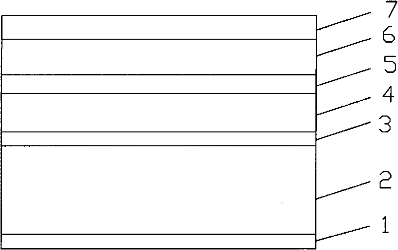
[0037] Such as Figure 1-4 Shown is the structure of a multi-junction solar cell with a Si / GaAs / InGaP three-layer structure. The bottom cell 1 is a Si PN junction cell, the middle cell 3 is a GaAs PN junction cell, and the top cell 5 is an InGaP PN junction cell. , Each sub-cell is directly grown on the silicon cell substrate.
[0038] Preparation method of multi-junction solar cell:
[0039] First, use 180μm thick P-type monocrystalline silicon to fabricate solar cells by chemical etching. The high-efficiency suede preparation is carried out in a magnetic field. That is, the monocrystalline silicon wafer is put into a suede preparation reactor equipped with a reaction solution. During the reaction, the suede preparation reactor is placed in a magnetic field below 15T. The ratio of the reaction solution is: sodium hydroxide or potassium hydroxide with a mass pe...
PUM
 Abstract
Description
Claims
Application Information


