Perovskite hybrid solar cell based on cadmium sulfide nanoarray
A nano-array and solar cell technology, applied in the field of solar cells, can solve problems such as departing from the original intention of solar cells, and achieve the effects of large-area preparation, simple process, and cost reduction
- Summary
- Abstract
- Description
- Claims
- Application Information
AI Technical Summary
Problems solved by technology
Method used
Image
Examples
Embodiment 1
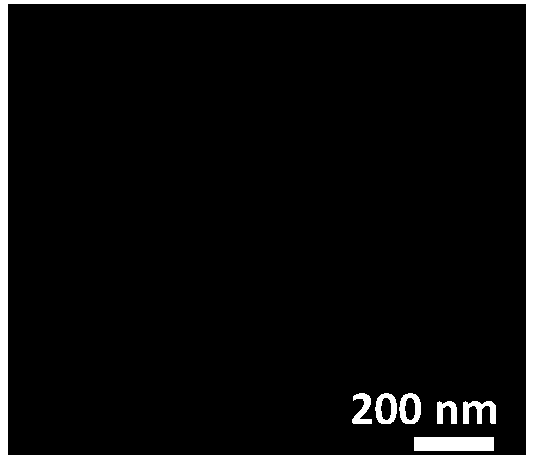
[0035] The glass substrate covered with indium tin oxide was ultrasonically washed with detergent, isopropanol, ethanol and acetone for 5 minutes, rinsed with deionized water and dried. CdS nanorod arrays were grown on the substrate by the sol-gel method, and the array height was 100 nm. After UV-ozone treatment, the CH with a thickness of 400 nm was prepared by solution spin coating. 3 NH 3 PB 3 The photosensitive layer is baked at 100°C for 15 minutes. in CH 3 NH 3 PB 3 2,2',7,7'-Tetrakis[N,N-bis(4-methoxyphenyl)amino]-9,9'-spirobifluorene A mixture of (spiro-MeOTAD), bis(trifluoromethylsulfonyl)lithium (Li-TFSI) and 4-tert-butylpyridine (TBP) at a molar ratio of 2.5:1:3 was used as a hole transport layer. Finally, a silver electrode with a thickness of 10 nm was prepared by vacuum evaporation. From image 3 It can be seen in the figure that the nanorods grow perpendicular to the ITO surface, with a length of about 400nm and a diameter of about 100nm. Such as fig...
Embodiment 2
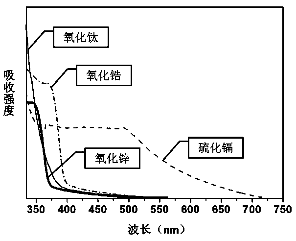
[0037] The glass substrate covered with fluorine-doped tin oxide was ultrasonically washed with detergent, isopropanol, ethanol and acetone for 5 minutes, rinsed with deionized water and dried. CdS nanowire arrays were grown on the substrate by the hydrothermal method, and the array height was 1000nm. After air heat treatment, CH with a thickness of 500nm was prepared by single-source vapor deposition. 3 NH 3 PbBr 3 The photosensitive layer is baked at 120° C. for 5 minutes. in CH 3 NH 3 PbBr 3 2,2',7,7'-Tetrakis[N,N-bis(4-methoxyphenyl)amino]-9,9'-spirobifluorene (spiro-MeOTAD), a mixture of bis(trifluoromethylsulfonyl)lithium (Li-TFSI) and 4-tert-butylpyridine (TBP) at a molar ratio of 2.5:1:3 as a hole transport layer. Finally, a 300 nm thick aluminum electrode was vacuum evaporated. Such as figure 2 As shown, the absorption spectrum of CdS nanoarrays to sunlight is wider than that of ZrO 2. As mentioned above, get as figure 1 The perovskite hybrid solar cell s...
Embodiment 3
[0039] The quartz substrate covered with fluorine-doped tin oxide was ultrasonically washed with detergent, isopropanol, ethanol, and acetone for 10 minutes, rinsed with deionized water and dried. The CdS nanotube array was grown on the substrate by electrochemical method, the array height was 500nm, after air heat treatment, the CH with a thickness of 30nm was prepared by dual-source vapor deposition method 3 NH 3 PBr 2 The photosensitive layer is baked at 140° C. for 10 minutes. in CH 3 NH 3 PBr 2 2,2',7,7'-Tetrakis[N,N-bis(4-methoxyphenyl)amino]-9,9'-spirobifluorene (spiro-MeOTAD), a mixture of bis(trifluoromethylsulfonyl)lithium (Li-TFSI) and 4-tert-butylpyridine (TBP) at a molar ratio of 2.5:1:3 as a hole transport layer. Finally, a 200nm thick magnesium electrode was prepared by vacuum evaporation. Such as figure 2 As shown, the absorption spectrum of CdS nanoarrays to sunlight is wider than that of TiO 2 . As mentioned above, get as figure 1 The perovskite ...
PUM
| Property | Measurement | Unit |
|---|---|---|
| height | aaaaa | aaaaa |
| thickness | aaaaa | aaaaa |
| thickness | aaaaa | aaaaa |
Abstract
Description
Claims
Application Information


