Ternary all-polymer solar cell
A solar cell and polymer technology, applied in circuits, photovoltaic power generation, electrical components, etc., can solve the problems of the research lag of non-fullerene electron acceptor materials, and achieve the improvement of photoelectric conversion performance, increase short-circuit current density, and inhibit dual The effect of molecular charge recombination
- Summary
- Abstract
- Description
- Claims
- Application Information
AI Technical Summary
Problems solved by technology
Method used
Image
Examples
Embodiment 1
[0031] Embodiment 1 (control group)
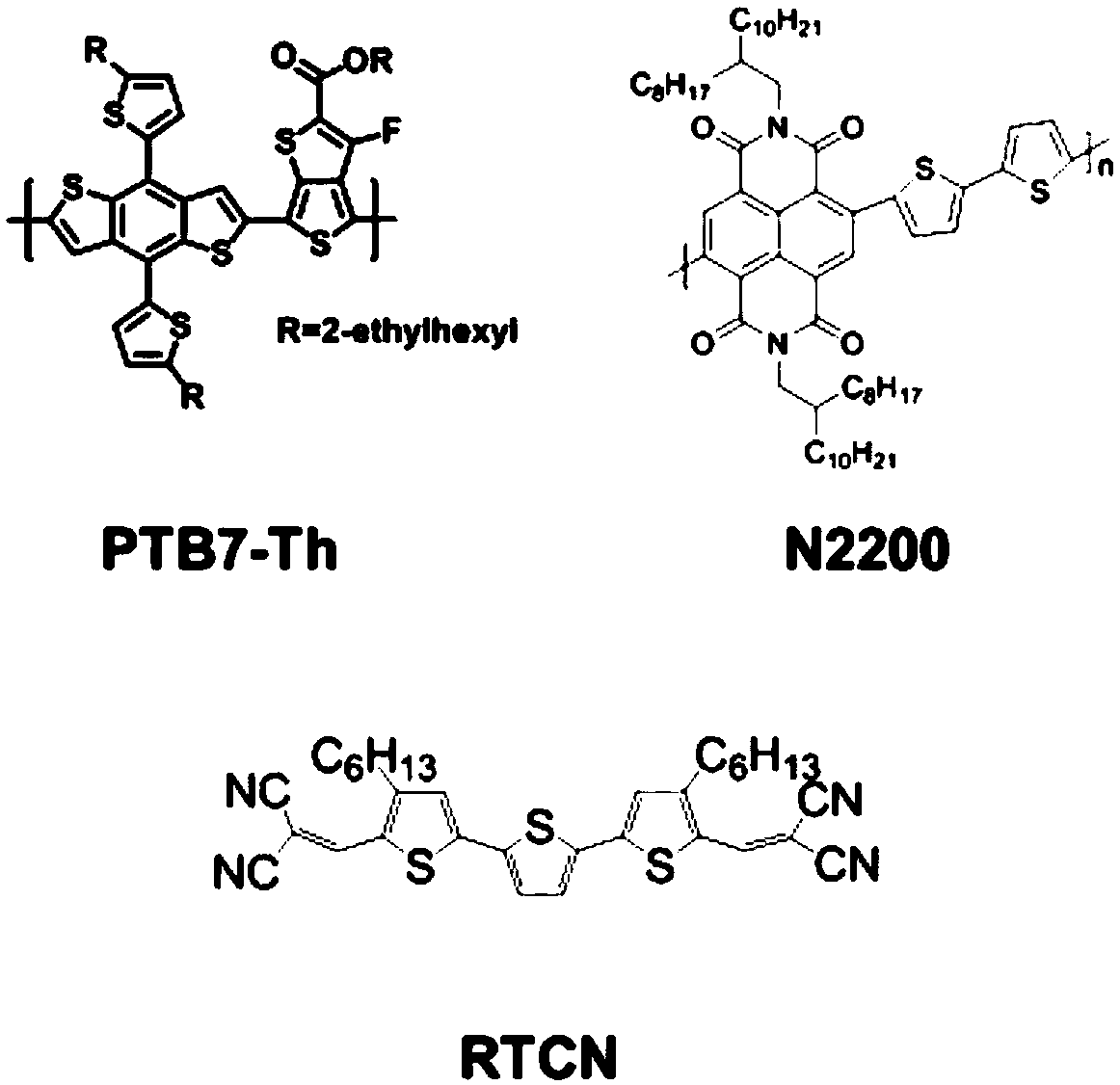
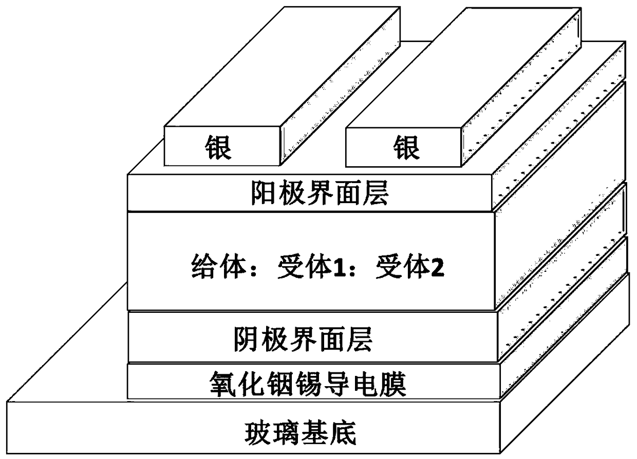
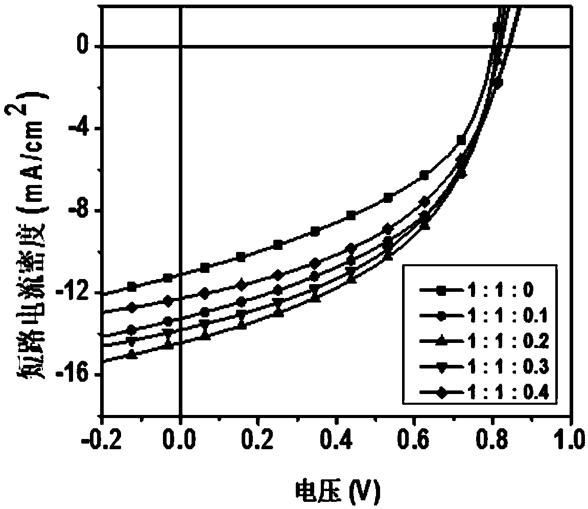
[0032]Clean the substrate composed of transparent substrate layer and transparent conductive cathode ITO with surface roughness less than 1nm, and blow dry with nitrogen after cleaning; spin-coat ZnO (4500rpm, 40s, 25nm) on the surface of transparent conductive cathode ITO to prepare cathode buffer layer, and the formed film was thermally annealed (200°C, 60min); the PTB7-Th:N2200 photoactive layer (2000rpm, 60s, 95nm) was prepared by spin coating on the cathode buffer layer, and the mass ratio was 1:1; Evaporation of MoO on the surface of the photoactive layer 3 (8nm); metal anode Ag (80nm) was vapor-deposited on the anode buffer layer. Under standard test conditions (AM1.5, 100mW / cm 2 ), the measured open circuit voltage of the device (V OC )=0.80V, short-circuit current (J SC )=11.1mA / cm 2 , fill factor (FF) = 0.45, photoelectric conversion efficiency (PCE) = 3.96%.
Embodiment 2
[0034] Clean the substrate composed of transparent substrate layer and transparent conductive cathode ITO with surface roughness less than 1nm, and blow dry with nitrogen after cleaning; spin-coat ZnO (4500rpm, 40s, 25nm) on the surface of transparent conductive cathode ITO to prepare cathode buffer layer, and the formed film was thermally annealed (200°C, 60min); the PTB7-Th:N2200:RTCN photoactive layer (2000rpm, 60s, 95nm) was prepared by spin coating on the cathode buffer layer, with a mass ratio of 1:1 :0.1; evaporate MoO on the surface of the photoactive layer 3 (8nm); metal anode Ag (80nm) was vapor-deposited on the anode buffer layer. Under standard test conditions (AM 1.5, 100mW / cm 2 ), the measured open circuit voltage of the device (V OC )=0.81V, short-circuit current (J SC )=13.1mA / cm 2 , fill factor (FF) = 0.47, photoelectric conversion efficiency (PCE) = 5.02%.
Embodiment 3
[0036] Clean the substrate composed of transparent substrate layer and transparent conductive cathode ITO with surface roughness less than 1nm, and blow dry with nitrogen after cleaning; spin-coat ZnO (4500rpm, 40s, 25nm) on the surface of transparent conductive cathode ITO to prepare cathode buffer layer, and the formed film was thermally annealed (200°C, 60min); the PTB7-Th:N2200:RTCN photoactive layer (2000rpm, 60s, 95nm) was prepared by spin coating on the cathode buffer layer, with a mass ratio of 1:1 :0.2; evaporate MoO on the surface of the photoactive layer 3 (8nm); metal anode Ag (80nm) was vapor-deposited on the anode buffer layer. Under standard test conditions (AM 1.5, 100mW / cm 2 ), the measured open circuit voltage of the device (V OC )=0.82V, short-circuit current (J SC )=13.6mA / cm 2 , fill factor (FF) = 0.48, photoelectric conversion efficiency (PCE) = 5.60%.
PUM
 Abstract
Description
Claims
Application Information


