Edge detection device and laser processing device

An edge detection device and laser processing technology, applied in measuring devices, laser welding equipment, optical devices, etc., can solve the problems of limited degree of freedom of configuration, high cost, troublesome setting of optical components and beam splitters, etc., and achieve freedom of configuration High-precision, high-precision effect

Inactive Publication Date: 2010-06-23
DISCO CORP
View PDF7 Cites 9 Cited by
  • Summary
  • Abstract
  • Description
  • Claims
  • Application Information

AI Technical Summary

Problems solved by technology

There is a problem that the hole for vacuuming formed in the workpiece holding area is blocked due to the attached dicing tape, or the surface accuracy of the workpiece holding area is lowered.
[0010] However, in the technique shown in Patent Document 2, since it is necessary to separately prepare the chuck table according to the shape of the workpiece, the cost is high, and the work of replacing the table is required.
[0011] In addition, in the conventional confocal detection device shown in Patent Document 3 and the like, as a spatial filter for guiding only light of a specific wavelength focused on the detection object out of white light to the spectroscope, A pinhole mask is used, but there is a problem that the accuracy of the spatial filter, the installation work of each optical component and the beam splitter are troublesome, and the degree of freedom of arrangement is limited.

Method used


Image

  • Edge detection device and laser processing device
  • Edge detection device and laser processing device
  • Edge detection device and laser processing device

Examples


Embodiment Construction

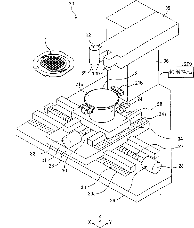
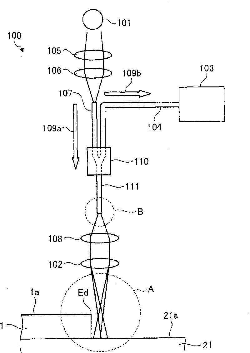
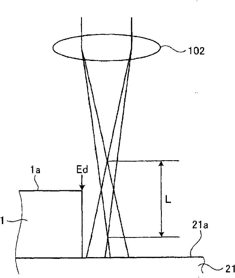
[0024] Hereinafter, an edge detection device of the best mode for carrying out the present invention and a laser processing device having the edge detection device will be described with reference to the drawings. The present embodiment shows an application example of a laser processing apparatus. The laser processing apparatus has an edge detection device for detecting semiconductors with devices formed in a plurality of regions divided by a plurality of partitions arranged in a grid. A workpiece such as a wafer is used as a detection target to detect its edge position, and the laser processing device irradiates a processing laser beam to the workpiece along a partition to perform laser processing.

[0025] figure 1 It is an external perspective view showing the main part of the laser processing apparatus according to the embodiment of the present invention. The laser processing apparatus 20 of this embodiment has a holding unit 21 having a holding surface 21a for holding the wo...


PUM

PropertyMeasurementUnit
diameteraaaaaaaaaa

Abstract

The invention provides a laser processing device and an edge detection device for precisely detecting an edge position of a detecting object having any shape and having a high precision and high degree of arranging freedom as a space light filter. The edge detection device is provided with a white light source (101) which is arranged for sending a white light with a plurality of wavelengths to a first light path (109a), a chromatic aberration collector lens (102) which forms a plurality of focal points on a light shaft of a detecting object (1) aiming at the wavelengths of the white light sent by the first light path (109a), a fiber (104) which is guided to a second light path (109b) different from the first light path (109a) by the white light reflected by the detecting object (1), and a detector (103) which is arranged for detecting the strength of the white light guided to the second light path (109b) by the fiber (104).

Description

Technical field [0001] The present invention relates to an edge detection device for detecting the edge of a detection target object, such as a semiconductor wafer, and a laser processing device having the edge detection device. Background technique [0002] In the semiconductor device manufacturing process, on the surface of a substantially disc-shaped semiconductor wafer, a plurality of areas are divided using spacers (cutting lines) arranged in a grid pattern, and ICs are formed in the divided areas ( Semiconductor wafers of circuits such as integrated circuits and LSIs (Large Scale Integrated Circuits) are cut along partitions and divided into individual circuits to manufacture individual semiconductor chips. The cutting of the semiconductor wafer along the spacer lane is generally performed using a cutting device called a cutter, but a processing method of cutting by irradiating a laser beam has also been tried (for example, refer to Patent Document 1). [0003] In order to p...

Claims


Application Information

Patent Timeline
Patent Type & Authority Applications(China)
IPC IPC(8): G01B11/00B23K26/00B23K26/03H01L21/68
Inventor 能丸圭司
Owner DISCO CORP
Why Eureka
Try Eureka