Infrared transparent conductive film and preparation method thereof
A transparent conductive thin film and thin film technology, applied in the field of material science, can solve the problems of not being able to significantly improve the optical performance and anti-electromagnetic interference performance of infrared detector window/hood materials
- Summary
- Abstract
- Description
- Claims
- Application Information
AI Technical Summary
Problems solved by technology
Method used
Image
Examples
Embodiment 1
[0018] The technical solution described in this embodiment is that a Cu thin film and a CuAlO thin film are sequentially covered on a sapphire substrate. The Cu thin film has a thickness of 300 nm and a refractive index of 1.07; the CuAlO thin film has a thickness of 170 nm and a refractive index of 1.70.
[0019] The concrete preparation process of this embodiment is:
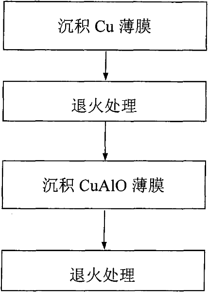
[0020] Step 1, using radio frequency magnetron sputtering method to deposit Cu thin film on sapphire substrate; the deposition process conditions are: sputtering power is 90W, Ar gas flow rate is 17.0SCCM, substrate temperature is 150°C, target base distance is 6.2 cm, the sputtering pressure is 0.5Pa, and the deposition time is 2.5h.
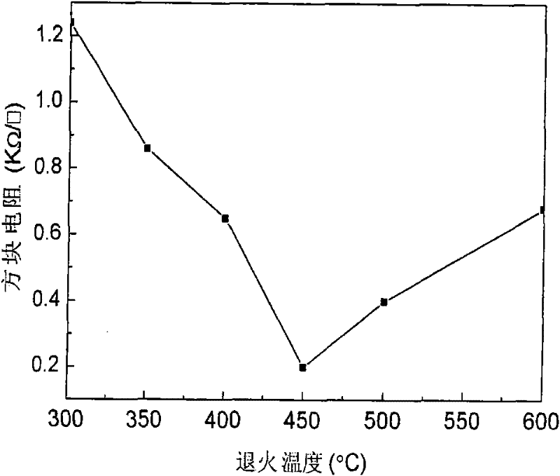
[0021] Step 2, annealing the sapphire with the Cu thin film deposited on the surface; the annealing process conditions are: the annealing temperature is 450°C, the annealing protective atmosphere is Ar gas, and the annealing time is 0.6h.
[0022] Step 3, using radio frequenc...
Embodiment 2
[0025] The technical solution described in this embodiment is that a Cu thin film and a CuAlO thin film are sequentially covered on a sapphire substrate. The Cu thin film has a thickness of 330 nm and a refractive index of 1.10; the CuAlO thin film has a thickness of 140 nm and a refractive index of 1.80.
[0026] The concrete preparation process of this embodiment is:
[0027] Step 1, using radio frequency magnetron sputtering method to deposit Cu thin film on sapphire substrate; the process conditions of deposition are: sputtering power is 80W, Ar gas flow rate is 19.0SCCM, substrate temperature is 200°C, target base distance is 6.5 cm, the sputtering pressure is 0.4Pa, and the deposition time is 3.0h.
[0028] Step 2, annealing the sapphire with the Cu thin film deposited on the surface; the annealing process conditions are: the annealing temperature is 500°C, the annealing protective atmosphere is Ar gas, and the annealing time is 0.5h.
[0029] Step 3, using radio frequ...
Embodiment 3
[0032] The technical solution described in this embodiment is that a Cu thin film and a CuAlO thin film are sequentially covered on a sapphire substrate. The Cu thin film has a thickness of 360 nm and a refractive index of 1.11; the CuAlO thin film has a thickness of 110 nm and a refractive index of 1.85.
[0033] The concrete preparation process of this embodiment is:
[0034] Step 1. Deposit a Cu thin film on a sapphire substrate by radio frequency magnetron sputtering; the deposition process conditions are: sputtering power is 73W, Ar gas flow is 21.0SCCM, substrate temperature is 240°C, and target base distance is 6.7 cm, the sputtering pressure is 0.3Pa, and the deposition time is 3.3h.
[0035]Step 2, annealing the sapphire with the Cu film deposited on the surface; the annealing process conditions are: the annealing temperature is 550°C, the annealing protective atmosphere is Ar gas, and the annealing time is 0.5h.
[0036] Step 3, using radio frequency magnetron sput...
PUM
| Property | Measurement | Unit |
|---|---|---|
| thickness | aaaaa | aaaaa |
| thickness | aaaaa | aaaaa |
| thickness | aaaaa | aaaaa |
Abstract
Description
Claims
Application Information


