
Method for preparing ZnO nanowire suspended back gate field-effect transistor

A technology of field effect tubes and nanowires, which is applied in semiconductor/solid-state device manufacturing, electrical components, circuits, etc., can solve problems such as no breakthrough results, and achieve the effects of simple process, high performance, and cost saving

Inactive Publication Date: 2010-06-23
INST OF MICROELECTRONICS CHINESE ACAD OF SCI
View PDF0 Cites 0 Cited by
  • Summary
  • Abstract
  • Description
  • Claims
  • Application Information

AI Technical Summary

Problems solved by technology

At present, some foreign researchers are trying to make E / D NW FETs in order to realize their application in logic circuits, but no breakthrough results have been achieved.

Method used


Image

  • Method for preparing ZnO nanowire suspended back gate field-effect transistor
  • Method for preparing ZnO nanowire suspended back gate field-effect transistor
  • Method for preparing ZnO nanowire suspended back gate field-effect transistor

Examples


Embodiment Construction

[0033] In order to make the object, technical solution and advantages of the present invention clearer, the present invention will be described in further detail below in conjunction with specific embodiments and with reference to the accompanying drawings.

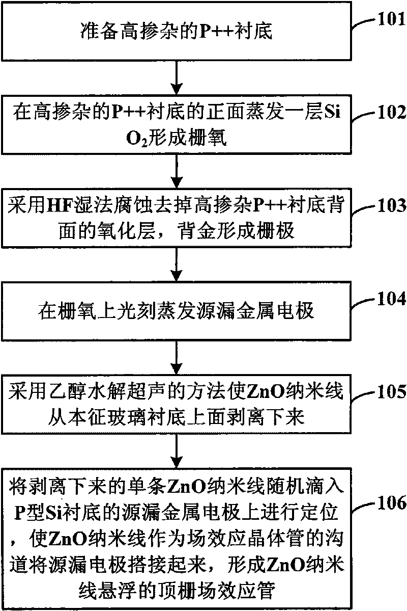
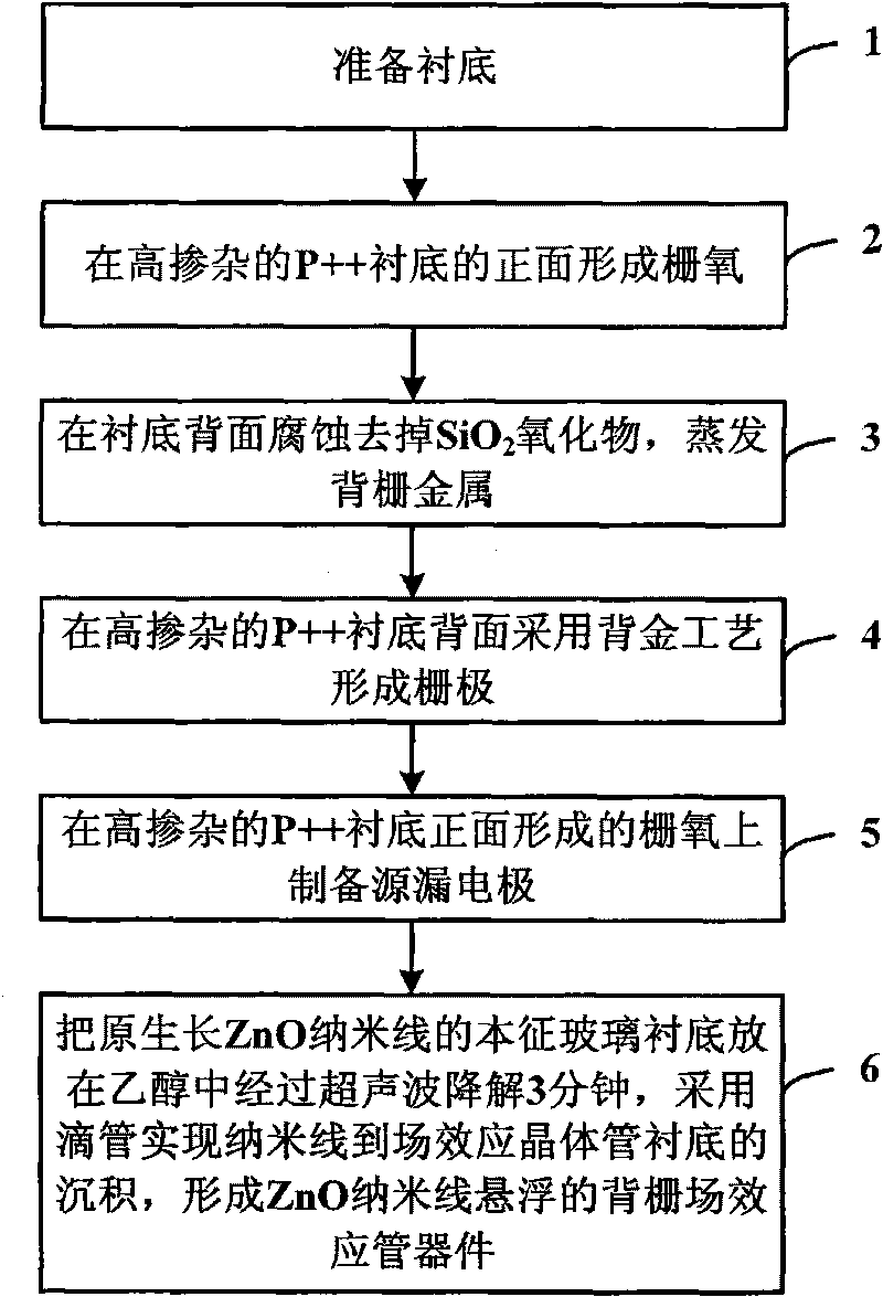
[0034] The core idea of ​​the present invention is: first prepare a highly doped P++ substrate, and evaporate a layer on the front side of the highly doped P++ substrate SiO 2 Form gate oxide, use HF to remove the oxide layer on the back of the highly doped P++ substrate, and form the gate with gold on the back; then photolithographically evaporate the source and drain metal on the gate oxide Electrodes, the ZnO nanowires are peeled off from the intrinsic glass substrate by the method of ethanol hydrolysis and ultrasound, and a single nanowire is randomly dropped onto the P-type Si substrate for positioning, so that the two ends of the nanowire overlap with the source and drain electrodes of the device , using ZnO nano...


PUM


Abstract

The invention discloses a method for preparing a ZnO nanowire suspended back gate field-effect transistor, comprising the following steps: preparing high-doped P + + substrate; evaporating a layer of SiO2 on the front of the high-doped P + + substrate to form gate oxide; adopting an HF wet method to corrode the oxide layer of the back of the high-doped P + + substrate, and forming grids on back gold; photoetching and evaporating source and drain metal electrodes on the gate oxide; adopting an ethanol hydrolysis ultrasound method to strip a ZnO nanowire from the upper surface of an intrinsic glass substrate; randomly dropping the stripped single-ZnO nanowire on the source and drain metal electrodes of a P-Si substrate for positioning, using the ZnO nanowires as the channels of the field-effect transistor to bond the source and drain metal electrodes, and forming the ZnO nanowire suspended back gate field-effect transistor. The method has the advantages of obvious effect, simple and easy process, economy and strong reliability, and is easily adopted and promoted in the preparation of microwave, millimeter wave compound semiconductor devices.

Description

technical field [0001] The invention relates to the technical field of compound semiconductor devices, in particular to a method for preparing a ZnO nanowire-suspended back gate field effect transistor. Background technique [0002] Nanowires (including nanotubes) are one of the most advanced topics in nanotechnology and condensed matter physics research. They have superior physical properties and are the structural units for constructing nanoscale components such as lasers, sensors, field-effect transistors, light-emitting diodes, logic circuits, spintronic devices, and quantum computers. Especially semiconductor nanowires, which can not only be used as basic building blocks, but also be used to connect various nanodevices. Through in-depth research on semiconductor nanowires, it is expected to prepare electronic, photon and spin information processing devices with complex functions on a single nanowire. [0003] In addition, a variety of composite nanomaterials can be sy...

Claims


Application Information

Patent Timeline
Patent Type & Authority Applications(China)
IPC IPC(8): H01L21/336
Inventor 黎明徐静波付晓君
Owner INST OF MICROELECTRONICS CHINESE ACAD OF SCI
Learn More