
Inorganic-pentacene like substance compound semiconductor material and preparation method thereof

A compound semiconductor and inorganic material technology, applied in semiconductor/solid-state device manufacturing, semiconductor devices, electric solid-state devices, etc., can solve the problems of low current intensity and low initial reduction potential, and achieve the effect of low cost and simple process

Inactive Publication Date: 2010-06-23
BEIJING UNIV OF CHEM TECH +1
View PDF0 Cites 4 Cited by
  • Summary
  • Abstract
  • Description
  • Claims
  • Application Information

AI Technical Summary

Problems solved by technology

However, the pentacene substances currently used in electronic devices are mostly limited to pure pentacene and its derivatives. Because pentacene substances are p-type semiconductors, the current intensity is small and the initial reduction potential is low at low potentials.

Method used


Image

  • Inorganic-pentacene like substance compound semiconductor material and preparation method thereof
  • Inorganic-pentacene like substance compound semiconductor material and preparation method thereof
  • Inorganic-pentacene like substance compound semiconductor material and preparation method thereof

Examples


Embodiment 1

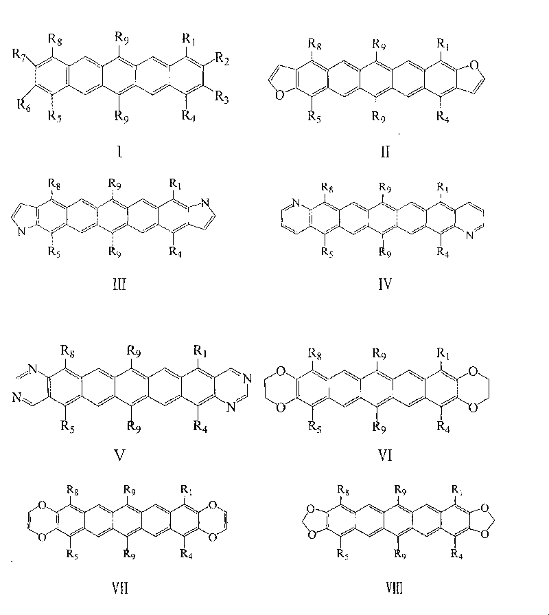
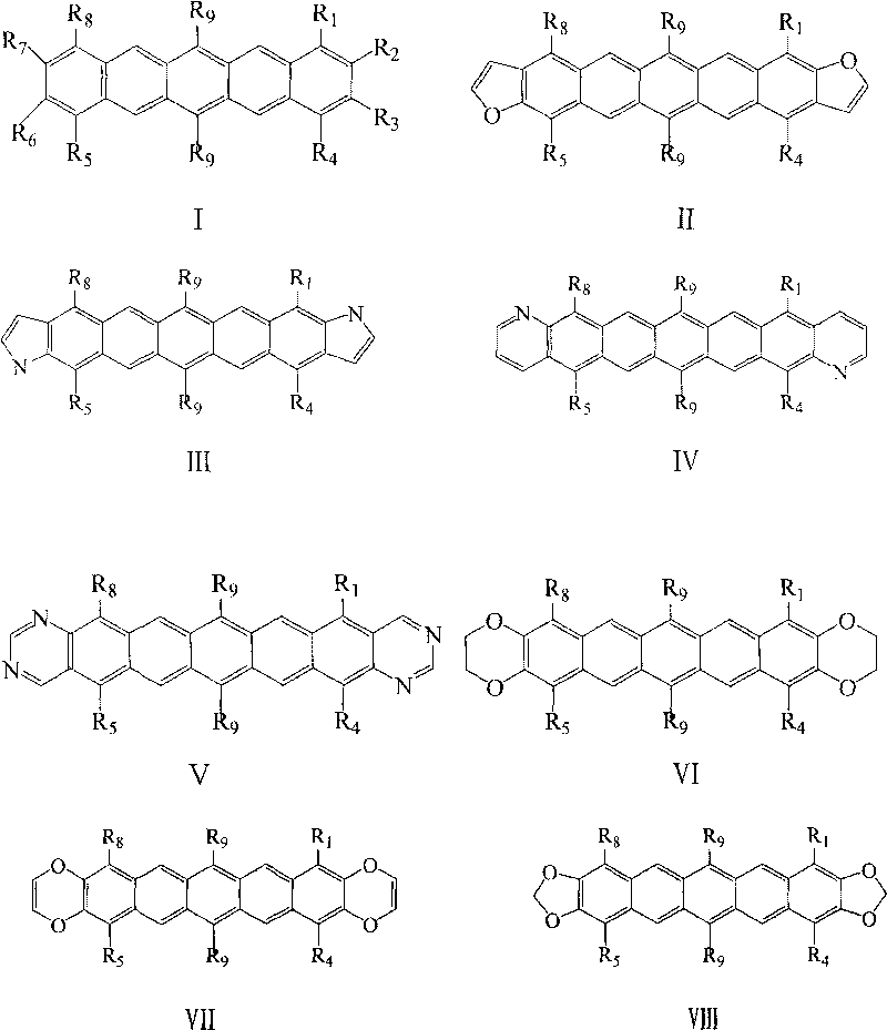
[0022] Nano-TiO 2 - Preparation of 6,13-bis(p-propylphenyl)pentacene composite material

[0023] Dissolve 334mg (0.625mmol) of 6,13-bis(p-propylphenyl)pentacene in 20mL of chloroform, and then add 10mg (0.125mmol) of TiO 2 (particle size is about 8nm), after sealing, at room temperature, ultrasonic dispersion for 3h, the resulting mixture is vacuum removed to obtain nano TiO 2 - 6,13-bis(p-propylphenyl)pentacene composite material.

Embodiment 2

[0025] Preparation of Nano ZnO-6,13-Diphenylpentacene Composite Material

[0026] Dissolve 284mg (0.626mmol) of 6,13-diphenylpentacene in 10mL of tetrahydrofuran, then add 25mg (0.313mmol) of ZnO (particle size is about 10nm), after sealing, ultrasonically disperse at room temperature for 6h, and the obtained The mixture was subjected to vacuum to remove the solvent to obtain nano ZnO-6,13-diphenylpentacene composite material.

Embodiment 3

[0028] Nano-TiO 2 - Preparation of 6,13-diphenylpentacene composite material

[0029] Dissolve 284mg (0.626mmol) of 6,13-diphenylpentacene in 20mL of chloroform, and then add 10mg (0.125mmol) of TiO 2 (particle size is about 8nm), after sealing, at room temperature, ultrasonic dispersion for 3h, the resulting mixture is vacuum removed to obtain nano TiO 2 - 6,13-diphenylpentacene composite material.


PUM


Abstract

The invention discloses an inorganic-pentacene like substance compound semiconductor material and a preparation method thereof. Pure pentacene and derivative thereof are applied on parts, which have small current intensity and low start and reduction potential when at the lower potential, of electronic devices. The inorganic-pentacene like substance compound semiconductor material prepared by the invention consists of pentacene like substance and inorganic material according to the molar ratio of 10:1-1:10. The invention removes organic solvent by dissolving the pentacene like substance into the organic solvent, adding the inorganic material according to the molar ratio of 10:1-1:10, sealing and dispersing for 0.5 to 10 hours, and then obtains the inorganic-pentacene like substance compound semiconductor material. The invention provides the compound semiconductor material which has both the advantages of n type semiconductors and p type semiconductors, has simple preparation method and low cost.

Description

technical field [0001] The invention belongs to the field of conductive materials, and in particular relates to an inorganic-pentacene compound semiconductor material and a preparation method thereof. Background technique [0002] The carrier mobility of pentacene substances in field effect transistors reaches 1.5cm 2 / (Vs) above, up to 5cm 2 / (Vs), is a research hotspot in the field of organic semiconductors. Inorganic nanomaterials exhibit small size effects, quantum size effects, surface and interface effects, and macroscopic quantum tunneling effects. When pentacene substances are compounded with inorganic nanomaterials, the atomic charge distribution, molecular packing mode, LUMO energy level, HOMO energy level, and bandgap width of the two materials will change. It has different properties from pentacene substances, and can be applied to fields such as field effect transistors, light-emitting diodes, and solar cells. For example, Minakata et al. observed as early a...

Claims


Application Information

Patent Timeline
Patent Type & Authority Applications(China)
IPC IPC(8): H01L51/00H01L51/30H01L51/40H01L51/46H01L51/48H01L51/54H01L51/56H10K99/00
CPCY02E10/50Y02E10/549
Inventor 张敬畅黄忠杨秀英曹维良
Owner BEIJING UNIV OF CHEM TECH
Learn More