Interdigital structure capable of regulating channel current of vertical gate SOI CMOS devices

A technology of channel current and vertical gate, which is applied in the direction of electric solid-state devices, semiconductor devices, semiconductor/solid-state device components, etc., can solve the problem of inability to design channel width vertical gate SOICMOS devices, etc., to improve the equivalent channel current , Improve the effect of gate width

Inactive Publication Date: 2010-06-30
SHANGHAI INST OF MICROSYSTEM & INFORMATION TECH CHINESE ACAD OF SCI +1
View PDF0 Cites 11 Cited by
  • Summary
  • Abstract
  • Description
  • Claims
  • Application Information

AI Technical Summary

Problems solved by technology

[0005] However, the channel length of the vertical gate SOI CMOS device structure can be extended by changing the layout, but the channel width is limited by the thickness of the top silicon, so there is a bottleneck in the design, that is, the maximum channel width is smaller than the top silicon of the SOI substrate. In this way, it is impossible to design a vertical gate SOI CMOS device with a relatively large channel width. For discrete or multiple SOI CMOS devices of the same type, the design purpose can be achieved by selecting a specific top silicon thickness, but if A variety of CMOS devices with different channel widths are involved in the circuit, the channel width must be easy to adjust, so as to achieve the purpose of adjusting the channel current of the vertical gate SOI CMOS device

Method used


Image

  • Interdigital structure capable of regulating channel current of vertical gate SOI CMOS devices
  • Interdigital structure capable of regulating channel current of vertical gate SOI CMOS devices
  • Interdigital structure capable of regulating channel current of vertical gate SOI CMOS devices

Examples


Embodiment 1

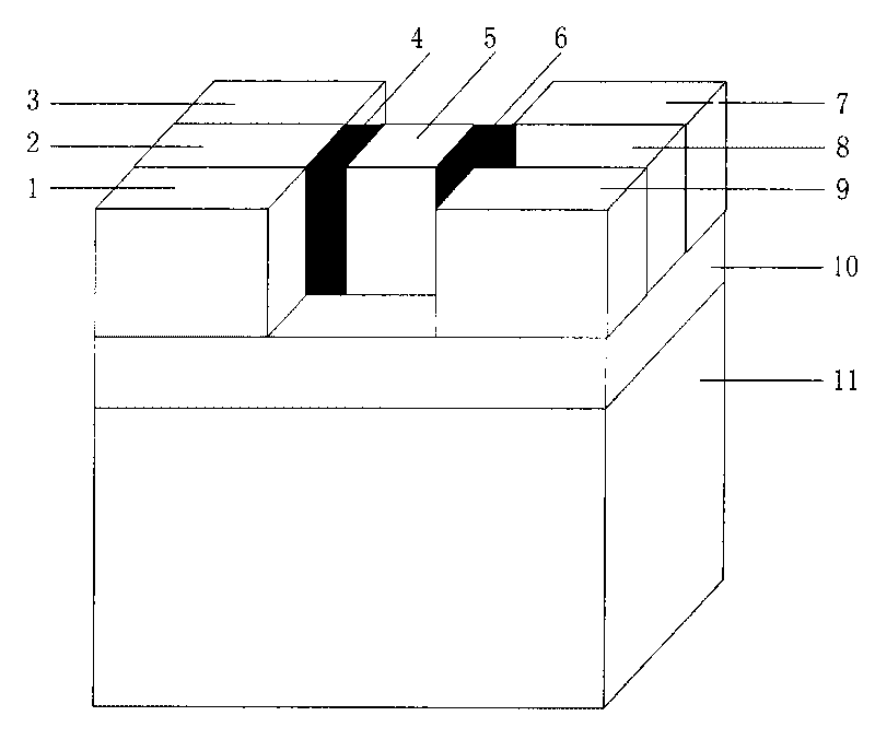
[0031] This embodiment provides an interdigital structure that can adjust the channel current of a vertical-gate SOI CMOS device, which is formed by arranging a plurality of vertical-gate SOI CMOS devices in parallel, wherein the PMOS regions of adjacent vertical-gate SOI CMOS devices are The PMOS area is adjacent, the NMOS area is adjacent to the NMOS area; the source area of ​​all vertical gate SOI CMOS devices is on the same side, and the drain area is on the other side; the gates of all vertical gate SOI CMOS devices are drawn from the side to form an interdigitated gate . Adjacent PMOS regions share one body electrode, and adjacent NMOS regions share one body electrode. All body electrodes are connected in parallel to form interdigital body electrodes. All sources drawn from the source region are connected in parallel to form an interdigitated source; all drains drawn from a drain region are connected in parallel to form an interdigitated drain.

[0032] The interdigitated ...

Embodiment 2

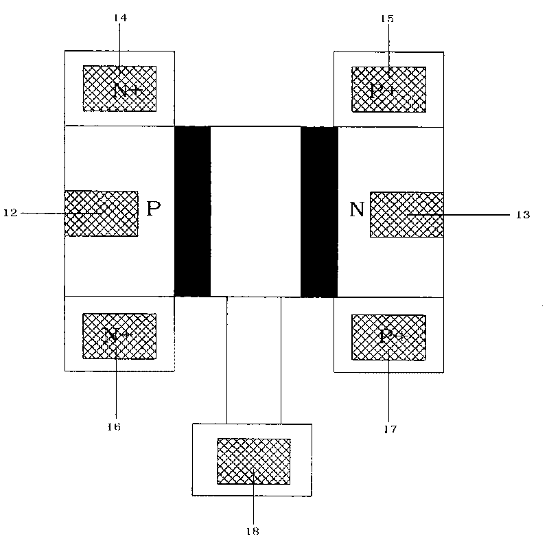
[0034] This embodiment provides an interdigital structure that can adjust the SOI CMOS channel current and increase the equivalent channel width, see image 3 . The structure includes an SOI substrate, multiple PMOS regions with P-channels, multiple NMOS regions with N-channels, and interdigital common gates; among them, PMOS and NMOS in the same CMOS share one gate, and multiple CMOS is distributed side by side and shares an interdigitated gate, and between adjacent CMOSs, NMOS and NMOS are in parallel, and PMOS and PMOS are in parallel. This interdigitated structure can solve the problem that the SOI CMOS vertical gate structure cannot adjust the gate width. It not only reflects the advantage of the SOI CMOS vertical gate structure to eliminate the floating body effect, but also can design different channel widths according to needs, and then design with different Channel current SOI CMOS vertical gate device.

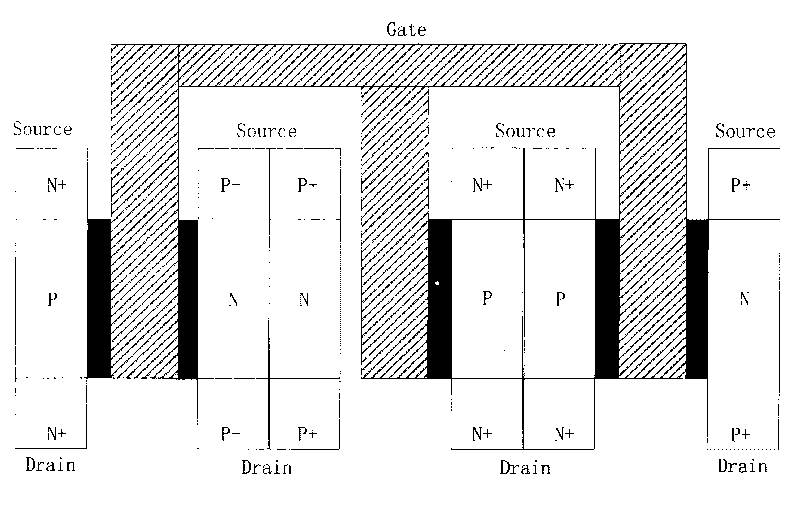
[0035] Such as Figure 4 As shown, the structural features of th...


PUM


Abstract

The invention discloses an interdigital structure capable of regulating the channel current of vertical gate SOI CMOS devices, which comprises a plurality of vertical gate SOI CMOS devices which are distributed in parallel, wherein PMOS regions of the adjacent vertical gate SOI CMOS devices are adjacent, and NMOS regions are also adjacent; source regions of all of the vertical gate SOI CMOS devices are positioned on the same side, and drain regions are positioned on the other side; and gate electrodes of all of the vertical gate SOI CMOS devices are led out of the side surface to form interdigital gate electrodes. The adjacent PMOS regions share one body electrode; the adjacent NMOS regions share one body electrode; and all of the body electrodes are connected in parallel to form an interdigital body electrode. All source electrodes led out from the source regions are connected in parallel to form an interdigital source electrode; and all drain electrodes led out from the drain regions are connected in parallel to form an interdigital drain electrode. In the invention, the gate electrodes of the plurality of the CMOS devices are connected in parallel by an interdigital topological structure, which is equivalent to improving the equivalent gate width of the vertical gate SOI CMOS devices so as to fulfill the aim of regulating the channel current of the vertical gate SOI CMOS devices.

Description

Technical field [0001] The invention belongs to the technical field of microelectronics and solid electronics, and relates to an interdigital structure capable of adjusting the channel current of a vertical gate SOI CMOS device. Background technique [0002] Silicon On Insulator (SOI) refers to the substrate technology that replaces the traditional bulk silicon substrate with an "engineered" substrate. This substrate usually consists of the following three layers: a thin single crystal silicon top layer on top An etching circuit is formed; a relatively thin buried oxide (BOX) layer, that is, an insulating silicon dioxide intermediate layer; a very thick bulk substrate silicon substrate layer, whose main function is to provide mechanical support for the upper two layers. Since the oxide layer in the SOI structure separates the silicon film layer on it from the silicon substrate layer, the large-area p-n junction will be replaced by dielectric isolation. The source region and drai...

Claims


Application Information

Patent Timeline
Patent Type & Authority Applications(China)
IPC IPC(8): H01L27/12H01L23/528H01L29/423
Inventor 程新红何大伟俞跃辉肖德元王中健徐大朋
Owner SHANGHAI INST OF MICROSYSTEM & INFORMATION TECH CHINESE ACAD OF SCI
Why Eureka
Try Eureka