Method for machining nanometer channel on microfluid chip

Inactive Publication Date: 2010-07-14
DALIAN MARITIME UNIVERSITY
View PDF0 Cites 12 Cited by
  • Summary
  • Abstract
  • Description
  • Claims
  • Application Information

AI Technical Summary

Problems solved by technology

[0005] 1. The process is complicated and the cost is high
For example, nanochannel processing methods based on electron beam lithography, coherent etching, and self-assembly have complex processing procedures, expensive processing equipment, and chips that cannot be reused many times, resulting in high processing costs.
[0006] 2. Nanochannels cannot be easily integrated with existing microfluidic chips, which limits the wide application of nanochannel technology
Existing nanochannel processing technology is difficult to integrate nanochannels into PDMS chips

Method used


Image

  • Method for machining nanometer channel on microfluid chip
  • Method for machining nanometer channel on microfluid chip
  • Method for machining nanometer channel on microfluid chip

Examples


Embodiment Construction

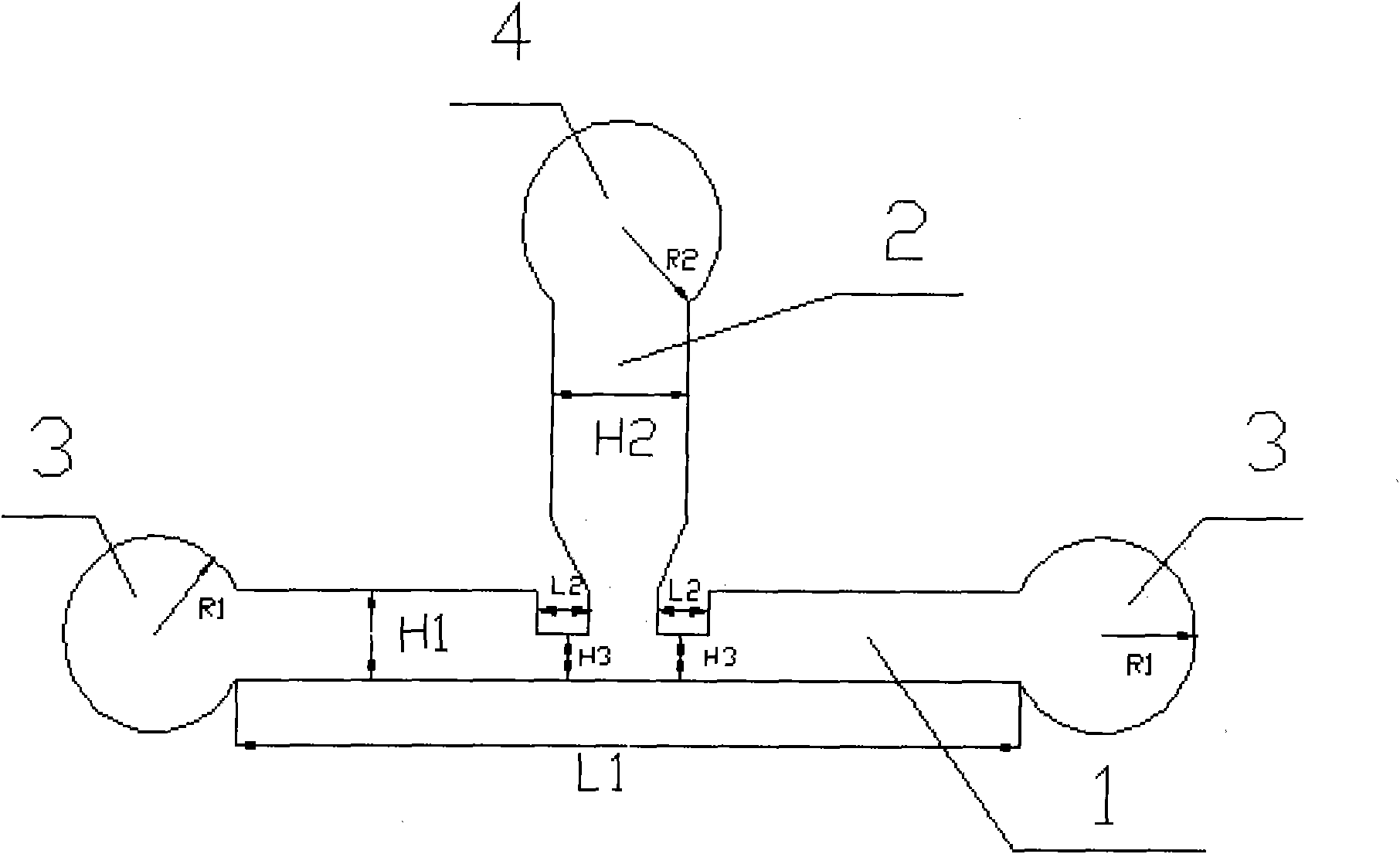
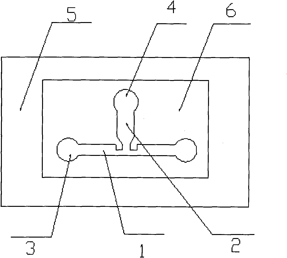
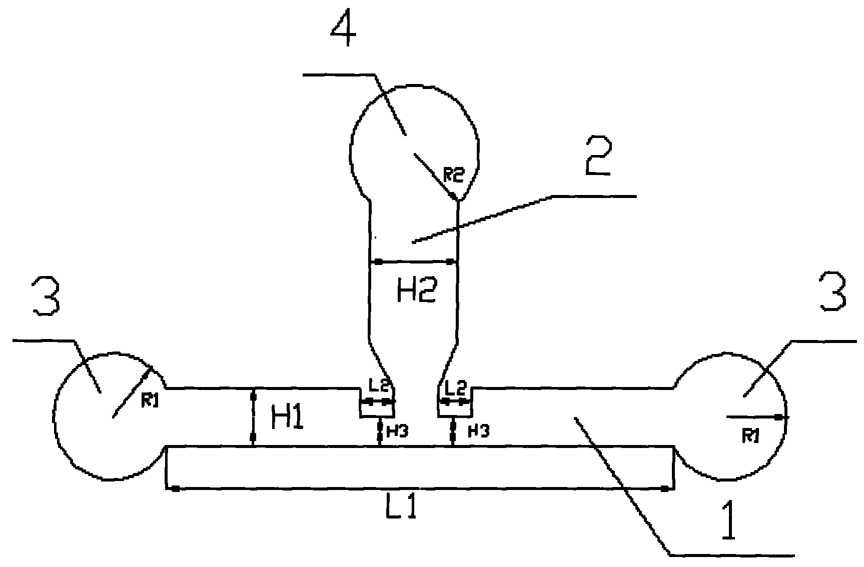
[0029] The present invention will be further described below in conjunction with the accompanying drawings. Such as Figure 1-2 As shown, a method for processing nanochannels on a microfluidic chip comprises the following steps:

[0030] A. Using lithography, that is, by printing a channel as a micron-scale mask, using SU-8 negative photoresist, and processing a main channel 1 and a mixed solution injection channel 2 on a silicon-based wafer by ultraviolet exposure Then cast polydimethylsiloxane (PDMS) on the wafer, and use a constant temperature vacuum furnace to cure for 3 to 4 hours at 70-80°C; peel off the PDMS from the wafer, and in the main channel 1 A buffer solution storage hole 3 is drilled at both ends of the buffer solution, and a mixed solution storage hole 4 is punched at the top of the mixed solution injection channel 2; the PDMS6 with the concave channel and the glass negative film 5 are sealed by air plasma. connected to form a chip with micron-scale channels...


PUM

PropertyMeasurementUnit
widthaaaaaaaaaa
widthaaaaaaaaaa
heightaaaaaaaaaa

Abstract

The invention discloses a method for machining a nanometer channel on a microfluid chip, which comprises the following steps of: firstly, producing a chip with a nanometer level channel of a mixed liquor injecting channel and a main channel; filling a mixed liquor-storing hole with mixed liquor of liquor PDMS with proper viscosity and curing agent; leading the mixed liquor to flow into the main channel along the mixed liquor injecting channel; immediately adding equal buffer solution into a buffer solution-storing hole when the distance from the mixed liquor to the lower wall surface of the main channel is 3-4mu m; slipping the cylinder-shaped PDMS into the mixed liquor-storing hole; sealing the mixed liquor-storing hole and the buffer solution-storing hole with transparent adhesive; and forming a nanometer level channel with a certain length at the lower wall surface closely near to the main channel after the PDMS is completely cured. The method is very simple, convenient and fast, can combine with different designs chip structures as required, realizes the nanometer channels with different structures, and naturally integrates the nanometer channels with the chip, thereby being a universal method.

Description

technical field [0001] The invention relates to the technical field of microfluidic chips, in particular to a method for processing nanometer channels on a microfluidic chip. Background technique [0002] Due to the size effect of the nanochannel structure, the specific surface area effect and the special physical and chemical properties inside and outside the pipeline, the nanochannel technology provides a new method in the detection and separation of chemistry and biomolecules. With the emergence of a variety of nanochannel processing technologies, some related technologies have gradually gained certain applications in many fields such as medicine, environmental monitoring, and homeland security. [0003] At present, the relatively mature nanochannel processing technologies mainly include: using natural channels, such as biomembrane ion channels; channels artificially synthesized with various materials, such as carbon nanotubes, arrayed nanochannels; and based on electron ...

Claims


Application Information

Patent Timeline
Patent Type & Authority Applications(China)
IPC IPC(8): B81C1/00
Inventor 宋永欣李冬青
Owner DALIAN MARITIME UNIVERSITY
Why Eureka
Try Eureka