Method for preparing GaN substrate with porous surface and GaN substrate prepared by using the method

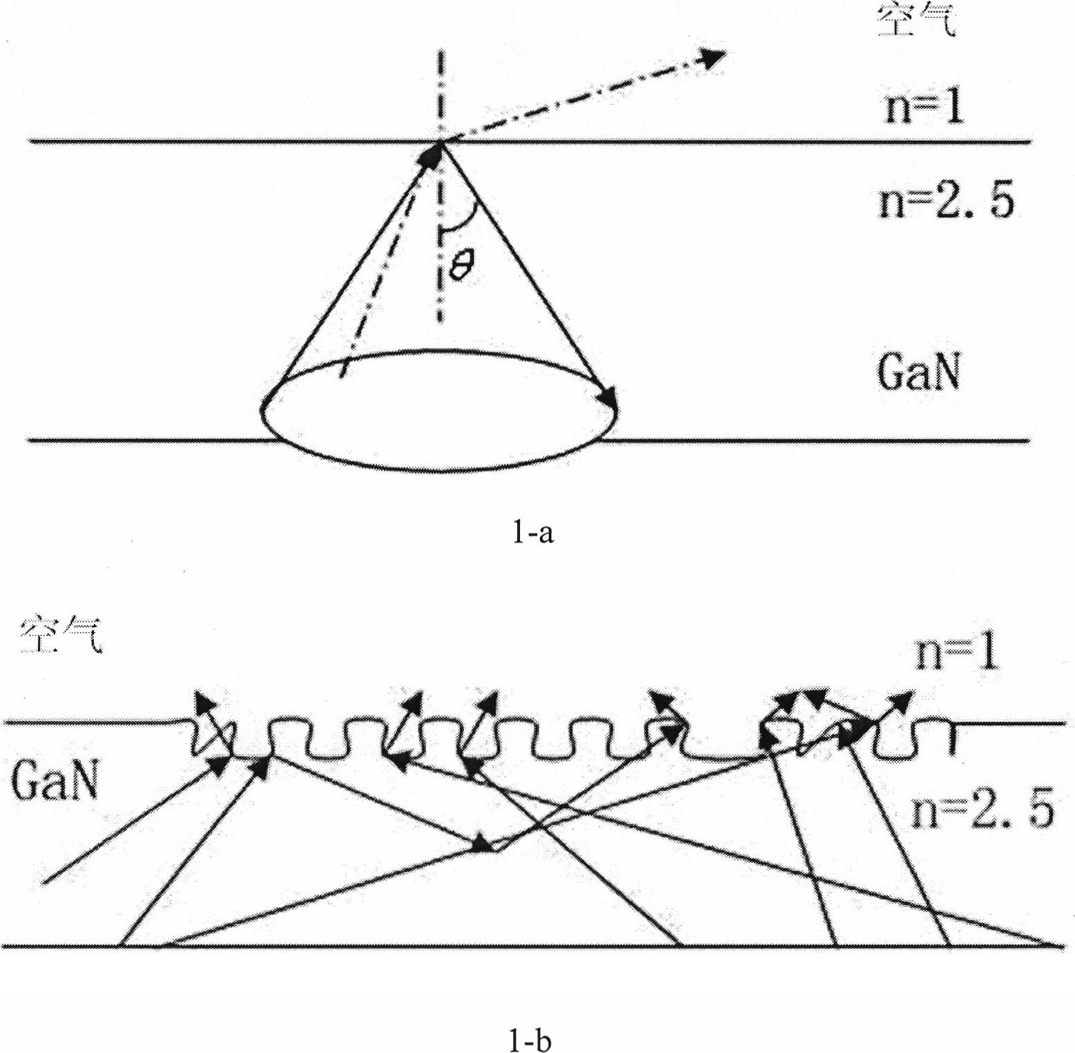
A technology with a porous surface and a substrate, which is applied in the direction of electrical components, circuits, semiconductor devices, etc., can solve the problems of not obtaining a porous structure, not proposing a process, and being simple, so as to improve the efficiency of light extraction and reduce the total reflection of the interface.

Inactive Publication Date: 2010-07-14
NANJING UNIV +1
View PDF0 Cites 16 Cited by
  • Summary
  • Abstract
  • Description
  • Claims
  • Application Information

AI Technical Summary

Problems solved by technology

[0005] Although scholars from various countries have carried out a lot of research on the surface nanostructure of GaN and the enhancement of light extraction efficiency by means of...

Method used


Image

  • Method for preparing GaN substrate with porous surface and GaN substrate prepared by using the method
  • Method for preparing GaN substrate with porous surface and GaN substrate prepared by using the method
  • Method for preparing GaN substrate with porous surface and GaN substrate prepared by using the method

Examples


Embodiment 1

[0035] The structure of the selected GaN substrate is as follows: a 30nm GaN low-temperature buffer layer is grown on the sapphire substrate material, and then an unintentionally doped n-type GaN layer is grown on the buffer layer with a thickness of 2.5 microns.

[0036] The preparation method of the porous GaN substrate comprises the following steps:

[0037] a. Clean the surface of the GaN substrate with acetone and alcohol respectively, put it in dilute hydrochloric acid and heat it to 40-70°C for 5-20 minutes, then wash it with deionized water, and wash it with N 2 Blow dry the surface. Then use electron beam evaporation technology to coat a layer of aluminum film with a thickness of 50-5000nm on the GaN layer on the surface of the GaN substrate;

[0038] b. place the GaN substrate covered with aluminum film on the surface in the acid solution (0.3M / L oxalic acid and 10% phosphoric acid mixed with a volume ratio of 1:1) in the electrochemical cell, the GaN substrate cove...

Embodiment 2

[0046] Adopt and the structure of the GaN substrate that example 1 selects for use, the preparation method of described superficially porous GaN substrate comprises the following steps:

[0047] a. Clean the surface of the GaN substrate with acetone and alcohol respectively, put it in dilute hydrochloric acid and heat it to 40-70°C for 5-20 minutes, then wash it with deionized water, and wash it with N 2 Blow dry the surface. Then use electron beam evaporation technology to coat a layer of aluminum film with a thickness of 500nm on the GaN layer on the surface of the GaN substrate;

[0048] b. place the GaN substrate covered with aluminum film on the surface in the acid solution (0.1M / L oxalic acid and 5% sulfuric acid mixed with a volume ratio of 1:1) in the electrochemical cell, the GaN substrate covered with aluminum film on the surface is Anode, graphite or Pt as the cathode, apply voltage to 60V, until the current is reduced to 0.1mA, anodic oxidation is realized by elec...

Embodiment 3

[0053] Adopt and the structure of the GaN substrate that example 1 selects for use, the preparation method of described superficially porous GaN substrate comprises the following steps:

[0054] a. Clean the surface of the GaN substrate with acetone and alcohol respectively, put it in dilute hydrochloric acid and heat it to 40-70°C for 5-20 minutes, then wash it with deionized water, and wash it with N 2 Blow dry the surface. Then use electron beam evaporation technology to coat a layer of aluminum film with a thickness of 500nm on the GaN layer on the surface of the GaN substrate;

[0055] b. place the GaN substrate covered with aluminum film on the surface in the acid solution (0.5M / L oxalic acid and 5% phosphoric acid mixed with a volume ratio of 1:1) in the electrochemical cell, the GaN substrate covered with aluminum film on the surface is Anode, graphite or Pt as the cathode, apply voltage to 60V, until the current is reduced to 0.1mA, anodic oxidation is realized by el...


PUM

PropertyMeasurementUnit
Thicknessaaaaaaaaaa
Thicknessaaaaaaaaaa

Abstract

The invention relates to a method for preparing a GaN substrate with a porous surface and a GaN substrate prepared by using the method. A porous structure is directly prepared on the surface of the GaN substrate by a wet etching method with simple process, low damage and high etching rate. The method for preparing a GaN substrate with a porous surface comprises the following steps of: a, plating a layer of aluminum film on the GaN layer on the surface of the GaN substrate; b, applying voltage in acid solution in an electrochemistry cell, and realizing anodic oxidation by an electrochemistry method so that the aluminum film becomes porous alumina; c, applying voltage continuously to 60-200V, etching the surface of the GaN substrate by the electrochemistry method and forming a porous structure on the surface of the GaN layer; and d, removing oxide on the surface to obtain the GaN substrate with a porous surface. In the invention, a disorder and porous structure on the surface of the GaNsubstrate is designed and prepared so that the optical propagation of the GaN-air interface is randomized, the total reflection of the interface is reduced to the maximum extent, and the light extraction efficiency is greatly improved.

Description

technical field [0001] The invention relates to a method for preparing a porous GaN substrate and the GaN substrate obtained by the preparation method, belonging to the field of semiconductor materials. Background technique [0002] Optoelectronic semiconductor devices play an increasingly important role in our life and scientific research. In recent years, nitride semiconductor light-emitting diodes (LEDs) based on gallium nitride (GaN) have been used more and more in practice, and high-efficiency blue LEDs have also been used as excitation light sources to achieve white light generation. illumination. As for the research and application of LED, people pay most attention to the internal quantum efficiency and external quantum efficiency of LED. Although the current internal quantum efficiency of GaN-based LEDs has reached 90%, due to total reflection at the interface between GaN and air, only no more than 12% of the light can escape from GaN and enter the air. This great...

Claims


Application Information

Patent Timeline
IPC IPC(8): H01L33/22
Inventor 张荣陈鹏谢自力施毅刘斌刘荣海于治国江若琏韩平修向前郑有炓
Owner NANJING UNIV
Why Eureka
Try Eureka