Control circuit for voltage dropping type power factor corrector

A technology of power factor correction and power factor correction, which is applied in the direction of output power conversion device, reactive power adjustment/elimination/compensation, AC power input conversion to AC power output, etc., can solve the problem of increased conduction loss of semiconductor devices, Input current power factor is difficult, diode reverse recovery loss and other problems, to reduce harmonic components, eliminate reverse recovery loss, reduce the effect of input current harmonics

Active Publication Date: 2010-07-14
INVENTRONICS HANGZHOU
View PDF0 Cites 67 Cited by
  • Summary
  • Abstract
  • Description
  • Claims
  • Application Information

AI Technical Summary

Problems solved by technology

However, the peak value of the current in the first control mode is very large, which increases the conduction loss of the semiconductor device and affects the efficiency.
The second control method can realize the current waveform close to the sine wave by rationally designing the slope of the compensation ramp wave, and its circuit system structure diagram is as follows figure 1 as shown, figure 2 is the input vol

Method used


Image

  • Control circuit for voltage dropping type power factor corrector
  • Control circuit for voltage dropping type power factor corrector
  • Control circuit for voltage dropping type power factor corrector

Examples


Embodiment Construction

[0032] The present invention will be further described in detail through specific examples and in conjunction with the accompanying drawings.

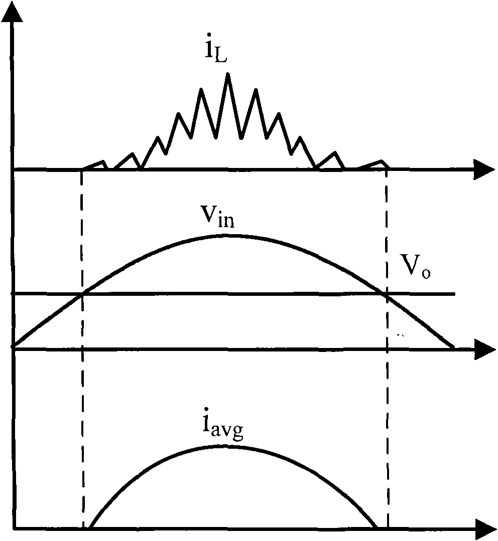
[0033] refer to Figure 4 , which is image 3 The main waveform diagram of the circuit shown, where Figure 4 (a) is the voltage V on C2 ramp with the error amplifier output voltage V EAO waveform diagram, Figure 4 (b) is the waveform diagram of Vgs driven by the switching tube. It can be seen from the figure that when V ramp voltage rises to V EAO , drive Vgs low. Figure 4 (c) is the current waveform of the switch tube, the current rises linearly when the switch tube is turned on, the current is zero when the switch tube is turned off, and the inductor current decreases linearly. Figure 4 (d) is the average value of the input current, that is, the switch current i Q average of.

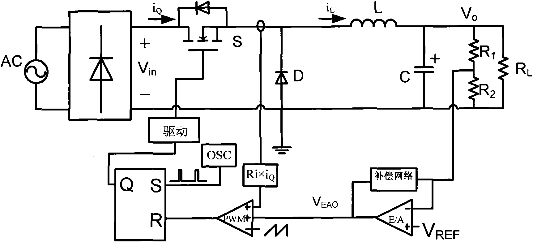
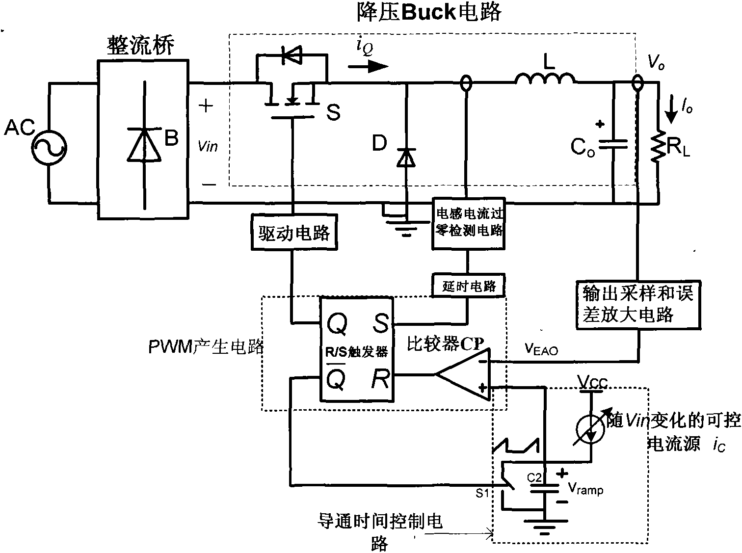
[0034] refer to Figure 5 , which is the specific circuit embodiment 1 of the present invention, the switch tube drive of the Buck circuit is pr...


PUM


Abstract

The invention discloses a control circuit for a voltage dropping type power factor corrector, which is used for controlling a voltage dropping converter to realize the power factor correction function. Inductance current critical intermittent control of changed on-time is performed on a Buck circuit through the control circuit to ensure that the on-time of a switching tube rises in the power frequency period along with increase of input voltage; and the critical intermittent working mode of inductance current in the Buck circuit is controlled, and when the inductance current is greater than zero, the junction capacitance of the switching tube and inductance are resonated, and the switching tube is connected when the voltage resonance of the junction capacitance reaches the volley bottom. The control circuit for the voltage dropping type power factor corrector has the characteristics of ensuring high power factors in the whole input voltage range, and meeting the harmonic requirements of IEC 61000-3-2 Class C, Class D, along with high efficiency.

Description

technical field [0001] The invention relates to a control circuit of a step-down power factor corrector, in particular to a step-down power factor correction circuit with high efficiency and low input current harmonics. Background technique [0002] Due to the presence of non-linear components and energy storage components in most electrical equipment at present, the input AC current waveform will be severely distorted, and the input power factor of the grid side is very low. In order to meet the harmonic requirements of the international standard IEC61000-3-2, A power factor correction (power factor correction, PFC) circuit must be added to these electric devices. Traditional active power factor correction circuits generally use a boost (Boost) topology, because the Boost topology is easy to control, simple to drive, and can perform switching operations during the entire power frequency cycle, and the power factor of the input current can be close to 1. The advantages. Ho...

Claims


Application Information

Patent Timeline
IPC IPC(8): H02J3/18H02J3/01H02M5/458
CPCY02E40/30Y02E40/40
Inventor 吴新科杨剑友张军明钱照明
Owner INVENTRONICS HANGZHOU
Why Eureka
Try Eureka