Method for reworking metal layer

A metal layer and heavy industry technology, applied in electrical components, semiconductor/solid-state device manufacturing, circuits, etc., can solve problems such as unsatisfactory results, metal surface erosion, chip scrapping, etc., to achieve the effect of improving the final yield

Inactive Publication Date: 2010-07-21
SEMICONDUCTOR MANUFACTURING INTERNATIONAL (BEIJING) CORP +1
View PDF0 Cites 9 Cited by
  • Summary
  • Abstract
  • Description
  • Claims
  • Application Information

AI Technical Summary

Problems solved by technology

The existing heavy industry technology is very easy to cause metal surface erosion and metal damage when removing the above defects, and brings more corrosion and metal damage defects while removing the original defects. Therefore, the risk of heavy industry failure is very high, and chips are often scrapped , the effect is very unsatisfactory (please refer to Figure 1a and Figure 1b , Figure 1a and Figure 1b Shown is a comparison of defect effects on wafers processed by prior art rework methods), so there is an urgent need for a rework method that can minimize the risk of rework wafers

Method used


Image

  • Method for reworking metal layer
  • Method for reworking metal layer
  • Method for reworking metal layer

Examples


Embodiment Construction

[0030] In order to better understand the technical content of the present invention, specific embodiments are given and described as follows in conjunction with the accompanying drawings.

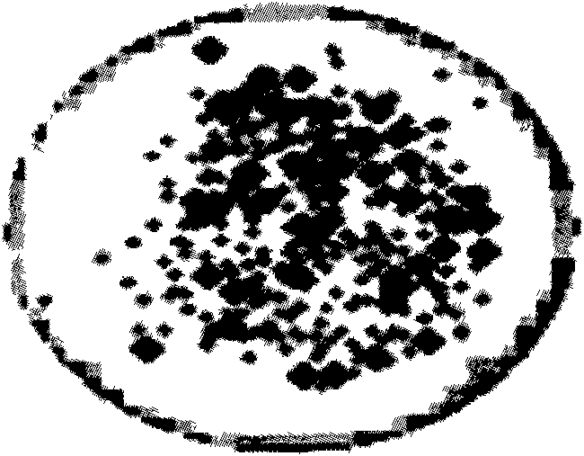
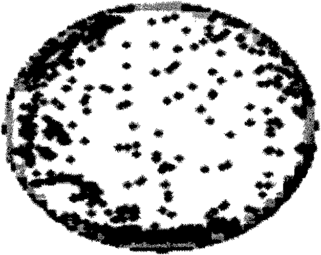
[0031] The invention proposes a metal layer rework method, which can greatly reduce metal residue defects, increase wafer output and reduce wafer scrapping.

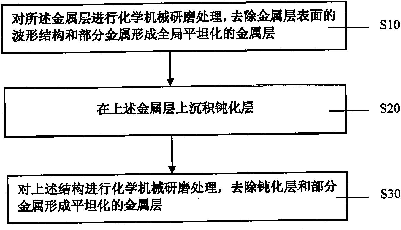
[0032] Please refer to figure 2 , figure 2 Shown is a flow chart of a metal layer reworking method in a preferred embodiment of the present invention. from figure 2 It can be seen that the present invention proposes a metal layer reworking method, which includes the following steps:

[0033] Step S10: performing chemical mechanical grinding on the metal layer, removing the corrugated structure and part of the metal on the surface of the metal layer to form a globally planarized metal layer;

[0034] Step S20: depositing a passivation layer on the metal layer;

[0035] Step S30: performing a chemical mechanical polishing proces...


PUM

PropertyMeasurementUnit
thicknessaaaaaaaaaa

Abstract

The invention provides a method for reworking a metal layer, which is applied in the field of integrated circuit manufacture. The method comprises the following steps: carrying out chemical mechanical lapping treatment on the metal layer, and removing a waveform structure and partial metal from the surface of the metal layer to form a globally planarized metal layer; depositing a passivation layer on the metal layer; and carrying out chemical mechanical lapping treatment on the structure, and removing the passivation layer and partial metal to form a planarized metal layer. The method for reworking the metal layer can greatly reduce surface defect caused by a normal chemical mechanical lapping process, such as the defects of metal, chemical, grinding fluid residue, microparticle residue and the like, even metal surface corrosion and crater defect, can remarkably improve the defect after the chemical mechanical lapping process, and increase the rate of good products.

Description

technical field [0001] The invention relates to the field of semiconductor product manufacturing, and in particular to a rework method applied in a chemical mechanical grinding process. Background technique [0002] The first time chemical mechanical polishing (CMP) was used in an interconnect process was in the planarization process of tungsten plug (WPlug) for Al interconnects. However, as the size of the device decreases and the structure becomes more and more complex, the disadvantages of aluminum wires become more and more obvious, including the increase of response delay (characterized by RC). Because copper has good electrical conductivity and excellent electromigration properties, copper interconnects have gradually replaced aluminum interconnects, and copper chemical mechanical polishing (CuCMP) has gradually attracted the attention of the industry. Generally, the copper damascene structure includes a semiconductor substrate, a dielectric layer is deposited on the ...

Claims


Application Information

Patent Timeline
Patent Type & Authority Applications(China)
IPC IPC(8): H01L21/321H01L21/3105B24B1/00
Inventor 李佩黄军平
Owner SEMICONDUCTOR MANUFACTURING INTERNATIONAL (BEIJING) CORP
Why Eureka
Try Eureka