Method for optimizing thickness of absorbing layer of indium antimonide photovoltaic detection device

A photovoltaic detector and indium photovoltaic technology, which is applied in the field of optimizing the thickness of the absorption layer of indium antimonide photovoltaic detector devices, can solve problems affecting device performance, achieve the effect of improving device performance and optimizing device design

Inactive Publication Date: 2010-08-04
SHANGHAI INST OF TECHNICAL PHYSICS - CHINESE ACAD OF SCI
View PDF0 Cites 9 Cited by
  • Summary
  • Abstract
  • Description
  • Claims
  • Application Information

AI Technical Summary

Problems solved by technology

However, its response is often restricted b

Method used


Image

  • Method for optimizing thickness of absorbing layer of indium antimonide photovoltaic detection device
  • Method for optimizing thickness of absorbing layer of indium antimonide photovoltaic detection device
  • Method for optimizing thickness of absorbing layer of indium antimonide photovoltaic detection device

Examples


Embodiment Construction

[0019] The specific embodiment of the present invention is described in detail below in conjunction with accompanying drawing:

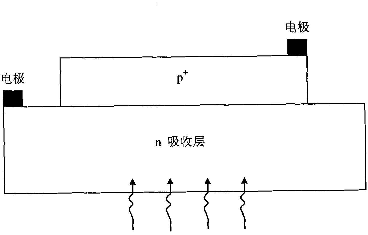
[0020] The device simulated by the present invention is a two-dimensional p + -on-n type indium antimonide photovoltaic detector device, the p-region doping concentration is 10 16 cm -3 , n-region doping concentration is 9×10 14 cm -3 , and passivate a layer of SiO on the entire outer surface of the device 2 , while electrodes are installed in the p-region and n-region respectively to measure the output voltage signal, see figure 1 .

[0021] The p-n junction photovoltaic detector is to make the p-n junction receive light irradiation to obtain energy. When light irradiates the p-n junction, the semiconductor in the junction and its vicinity absorbs light energy, electrons in the valence band are stimulated to transition to the conduction band to form free electrons, and correspondingly form free holes in the valence band. These minority carrier...


PUM


Abstract

The invention discloses a method for optimizing the thickness of the absorbing layer of an indium antimonide photovoltaic detection device. The method is that a spectral response curve under different thickness of the absorbing layer when light is irradiated in an absorbing area is obtained through device simulation, the obtained thickness of the absorbing layer corresponding to the maximum spectral response value is the optimum thickness of the absorbing layer through comparing with the spectral response data measured by experiments, and basis is further provided for the optimization of the thickness of the absorbing layer of the indium antimonide photovoltaic detection device. The invention has very great significance to the improvement of the device performance and the optimization of the device design.

Description

technical field [0001] The invention relates to semiconductor photodetection device technology, in particular to a method for optimizing the thickness of an absorption layer of an indium antimonide photovoltaic type detection device. Background technique [0002] Infrared photoelectric detection technology has achieved rapid development in the 1990s, and now it has developed into a large-scale focal plane array imaging technology. High-performance large-scale focal plane arrays have been formally used in various major national security projects. The indium antimonide detector responds in the 3-5 μm band, and because it is intrinsic absorption, the quantum efficiency is high. In the 1990s, the indium antimonide infrared focal plane array device developed maturely, and its development was mainly based on the staring type, which occupied a dominant position in the staring military system. Staring at the indium antimonide infrared focal plane has formed different technical char...

Claims


Application Information

Patent Timeline
IPC IPC(8): H01L31/18
CPCY02P70/50
Inventor 胡伟达郭楠陈效双陆卫
Owner SHANGHAI INST OF TECHNICAL PHYSICS - CHINESE ACAD OF SCI
Why Eureka
Try Eureka