

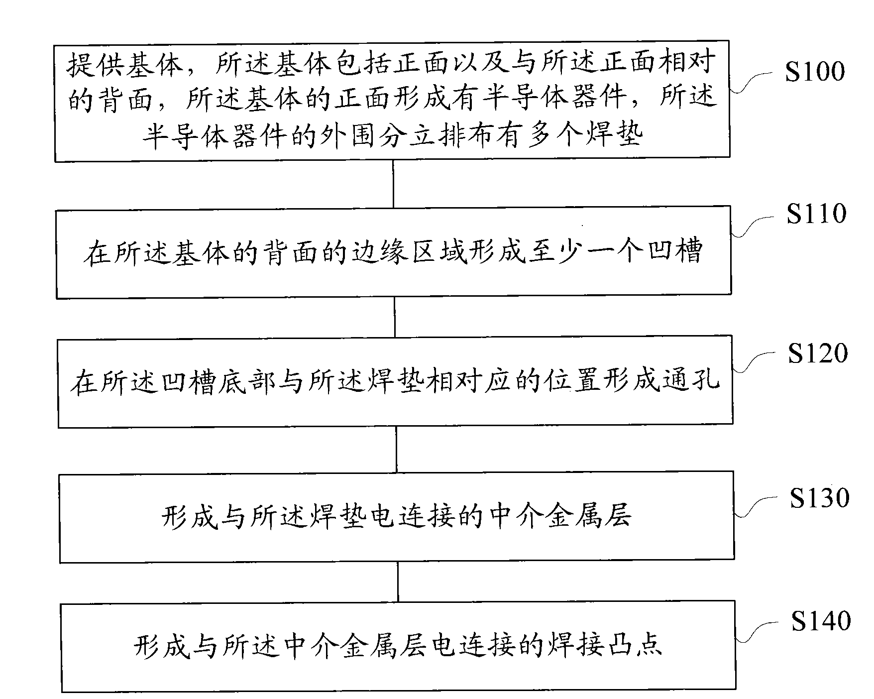
Packaging structure of semiconductor device and manufacture method thereof
A technology of packaging structure and manufacturing method, which is applied in the direction of semiconductor/solid-state device manufacturing, semiconductor devices, semiconductor/solid-state device components, etc., can solve problems such as chip electrical performance failure, long working hours, and difficult deposition of side walls of through holes, etc. To achieve the effect of improving reliability, small size and changing size
- Summary
- Abstract
- Description
- Claims
- Application Information
AI Technical Summary
Problems solved by technology
Method used
Image

Examples
no. 1 example
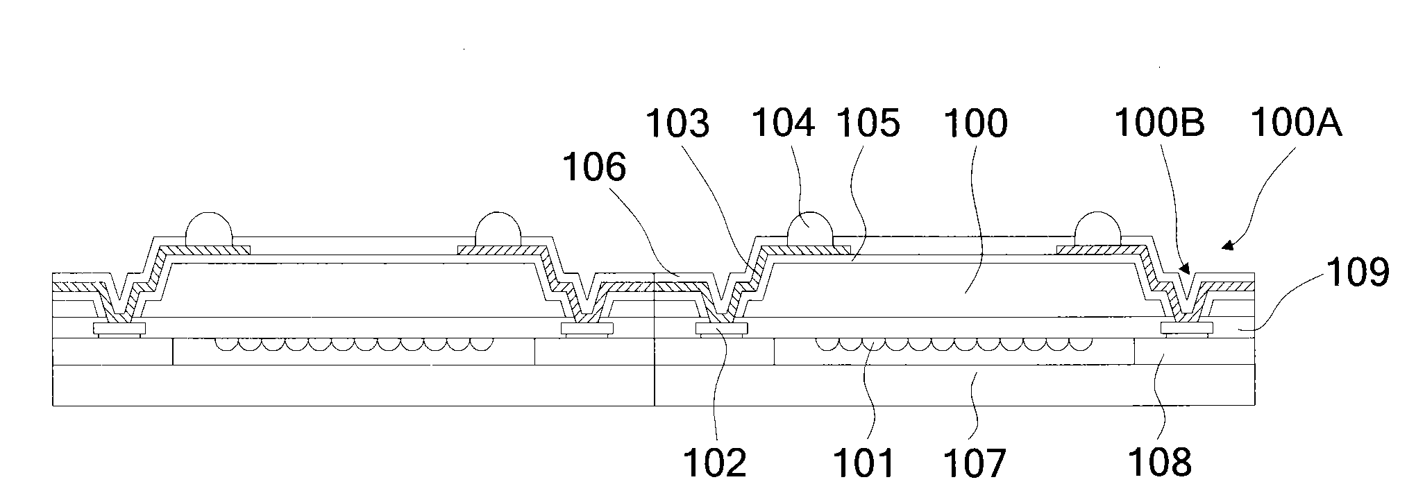
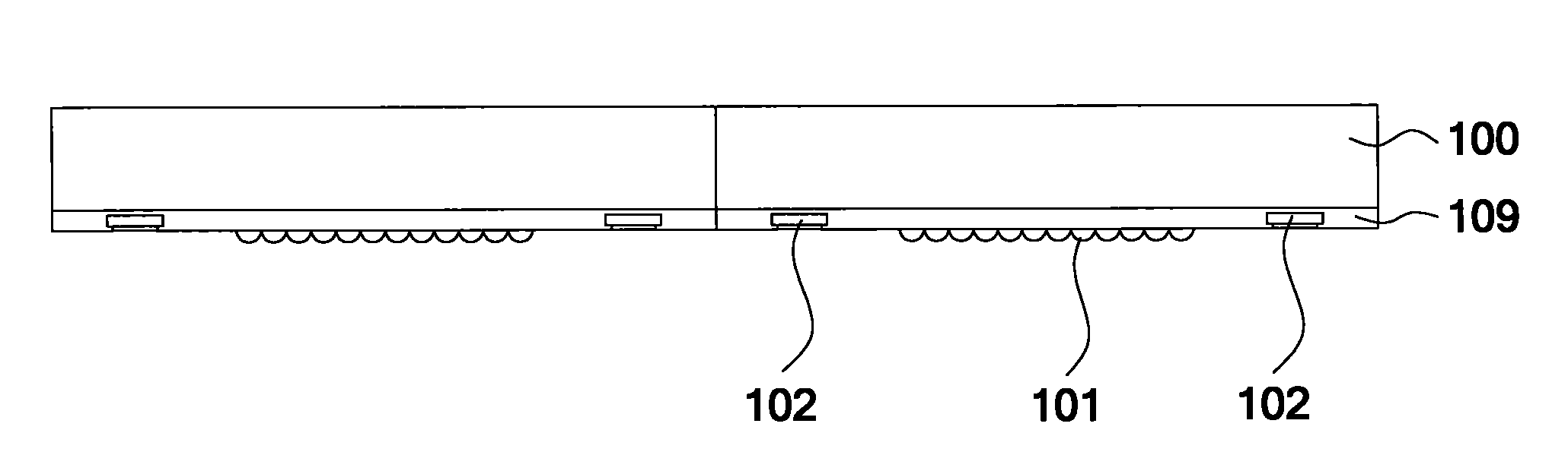
[0039] Please refer to figure 1 , which is a schematic cross-sectional view of the package structure of the semiconductor device provided in the first embodiment of the present invention, as figure 1As shown, the packaging structure of the semiconductor device includes: a substrate 100 , a semiconductor device 101 , a pad 102 , a groove 100A, a through hole 100B, an intermediary metal layer 103 , and a solder bump 104 . Wherein, the substrate 100 includes a front surface and a back surface opposite to the front surface, the semiconductor device 101 is located on the front surface of the substrate 100, and a plurality of welding pads 102 are discretely arranged on the periphery of the semiconductor device 101, and the function of the welding pads 102 is to form a semiconductor device 101 An interconnection connection point between an internal circuit and an external circuit. The groove 100A is located at the edge region of the back surface of the substrate 100, and the through...
no. 2 example
[0068] The difference between this embodiment and the first embodiment is that the packaging structure of the semiconductor device provided by this embodiment has multiple grooves, and the bottom of each groove is provided with multiple through holes.
[0069] In this implementation, the substrate 200 is a square, and the groove can be formed through the following steps: first, as Figure 14 As shown, a first etching region A15 is selected at each edge position of the base body 200, and the first etching step is performed from the back side of the base body 200 to form four grooves, and the four grooves are located on the sides of the base body 200 respectively. On the four edge regions, the solder pads are not exposed after the first etching step;
[0070] Next, if Figure 15 As shown, a plurality of second etching regions A20 are selected at the bottom of each first etching region A15, and the second etching regions A20 correspond to the pads one by one, and a second etchin...
no. 3 example
[0072] The difference between this embodiment and the previous two embodiments is that the packaging structure of the semiconductor device has only one groove, and the bottom of the groove is provided with a plurality of through holes.
[0073] Specifically, the groove can be formed through the following steps: first, as Figure 16 As shown, the edge region A25 of the back side of the substrate 300 is mechanically half-cut to form a groove, and the groove does not expose the pad;
[0074] Next, if Figure 17 As shown, a second etching step is performed on the back side of the substrate 300 corresponding to the welding pad (that is, the second etching region A30) to form a plurality of through holes at the bottom of the groove, so as to ensure that the surface of the welding pad is removed. After the passivation layer, the solder pad can be exposed.
PUM
 Abstract
Description
Claims
Application Information