Packaging structure of semiconductor element and manufacture method thereof

A technology of packaging structure and manufacturing method, which is applied in semiconductor/solid-state device manufacturing, semiconductor devices, semiconductor/solid-state device components, etc., can solve problems such as long working hours, chip electrical performance failure, and a chip electrical performance failure, etc., to achieve Effects of improving yield rate and improving reliability

Active Publication Date: 2010-08-11
CHINA WAFER LEVEL CSP
View PDF4 Cites 24 Cited by
  • Summary
  • Abstract
  • Description
  • Claims
  • Application Information

AI Technical Summary

Problems solved by technology

This process flow can effectively achieve high-density three-dimensional via interconnection, but there are the following problems: First, there is only a very thin insulating layer between the wafer and the copper layer, which leads to the interconnection of TSV A very high capacitance is formed between them, sometimes even exceeding the capacitance value of the traditional wire bonding interconnection; and, a thicker copper layer is filled in the silicon hole, due to the large gap between the silicon and the copper thermal mismatch, which can lead to significant thermal stress during thermal cycling; and, it is also necessary to overcome the void or seam phenomenon generated when electroplating copper; in addition, electroplating copper is used to completely fill The silicon hole method requires a long man-hour, which increases the production cost
[0004] The Chinese patent application number 200810178977.7 discloses a wafer-level chip packaging method and packaging structure, which can increase the connection area between the intermediary metal layer and the pad. The size of the bottom of the through hole is usually 50-60um. Since the size of the opening of the through hole is extremely small, and the depth of the through hole is relatively large, the opening of the through hole is very easy to Blocked by insulating material or metal, it is difficult to deposit the sidewall of the via hole on the insulating material and the intervening metal layer, and a chip usually has dozens of via holes, as long as the sidewall of one of the via holes is not deposited on Insulating materials or intervening metal layers, or unsatisfactory deposition effects, will lead to a chip electrical failure. For wafer-level chip size packaging, a wafer has thousands of chips, and the probability of chip electrical failure magnified hundreds of times

Method used


Image

  • Packaging structure of semiconductor element and manufacture method thereof
  • Packaging structure of semiconductor element and manufacture method thereof
  • Packaging structure of semiconductor element and manufacture method thereof

Examples


Embodiment Construction

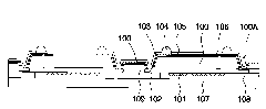
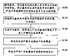
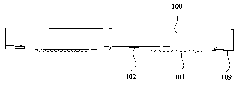
[0027] In the present invention, after the through hole is formed, part of the matrix is ​​removed so that the thickness of the matrix around the through hole is smaller than the thickness of the matrix inside the through hole, thereby making the depth of the through hole smaller, which can ensure that the opening of the through hole is not easily formed. The accumulation of metal or insulating materials greatly improves the yield rate of the process, thereby improving the reliability of the product, and is conducive to large-scale production.

[0028] The packaging structure and manufacturing method of the semiconductor device of the present invention will be described in more detail below in conjunction with schematic diagrams, wherein a preferred embodiment of the present invention is represented, it should be understood that those skilled in the art can modify the present invention described here, and still realize the present invention Beneficial effects of the invention. ...


PUM


Abstract

The invention discloses a packaging structure of a semiconductor element and a manufacture method thereof, wherein the packaging structure of the semiconductor element comprises a base body, a semiconductor element, a plurality of welding pads, through holes, a dielectric metal layer and a solder bump, wherein the base body comprises a front face and a back face opposite to the front face; the semiconductor element is positioned on the front face of the base body; the welding pads are positioned on the front face of the base body and are respectively distributed at the periphery of the semiconductor element; the through holes are positioned in the back face of the base body and correspond to the welding pads; the dielectric metal layer is electrically connected with the welding pads; the solder bump is electrically connected with the dielectric metal layer; and the thickness of the base body at the periphery of the through holes is smaller than that of the base body at the inner side of the through holes, which prevents insulating materials or metal from being accumulated in the openings of the through holes, improves the reliability of products, and reduces the size of the packaging structure.

Description

technical field [0001] The invention relates to the field of semiconductor packaging, in particular to a wafer-level chip packaging structure and a manufacturing method of a semiconductor device. Background technique [0002] Wafer-level chip-scale packaging usually distributes solder pads arranged on the periphery of a semiconductor chip into a large number of metal solder balls arranged in an area array through a redistribution process, and the metal solder balls are also called solder bumps. Since wafer-level chip size packaging is first packaged and tested on the entire wafer, and then cut, it has more obvious advantages: First, the process is greatly optimized, and the wafer directly enters the packaging process, while the traditional process is before packaging. It is necessary to cut and classify the wafers; and, the wafer-level chip size package is a one-time package of all integrated circuits, the marking work is carried out directly on the wafer, and the package te...

Claims


Application Information

Patent Timeline
Patent Type & Authority Applications(China)
IPC IPC(8): H01L23/485H01L21/60
CPCH01L24/11H01L2224/11H01L2924/12041H01L2924/14H01L2924/351H01L2924/00H01L2924/00012
Inventor 王之奇俞国庆邹秋红王文斌王蔚
Owner CHINA WAFER LEVEL CSP
Why Eureka
Try Eureka