

Method for directionally solidifying and purifying polycrystalline silicon under DC electric field
A technology of directional solidification and DC electric field, applied in the growth of polycrystalline materials, chemical instruments and methods, single crystal growth, etc., can solve the problems of increasing difficulty, no purification effect of impurities, etc., and achieve the effect of low content of crystal impurities
Inactive Publication Date: 2010-08-25
上海太阳能电池研究与发展中心
View PDF7 Cites 9 Cited by
- Summary
- Abstract
- Description
- Claims
- Application Information
AI Technical Summary
Problems solved by technology
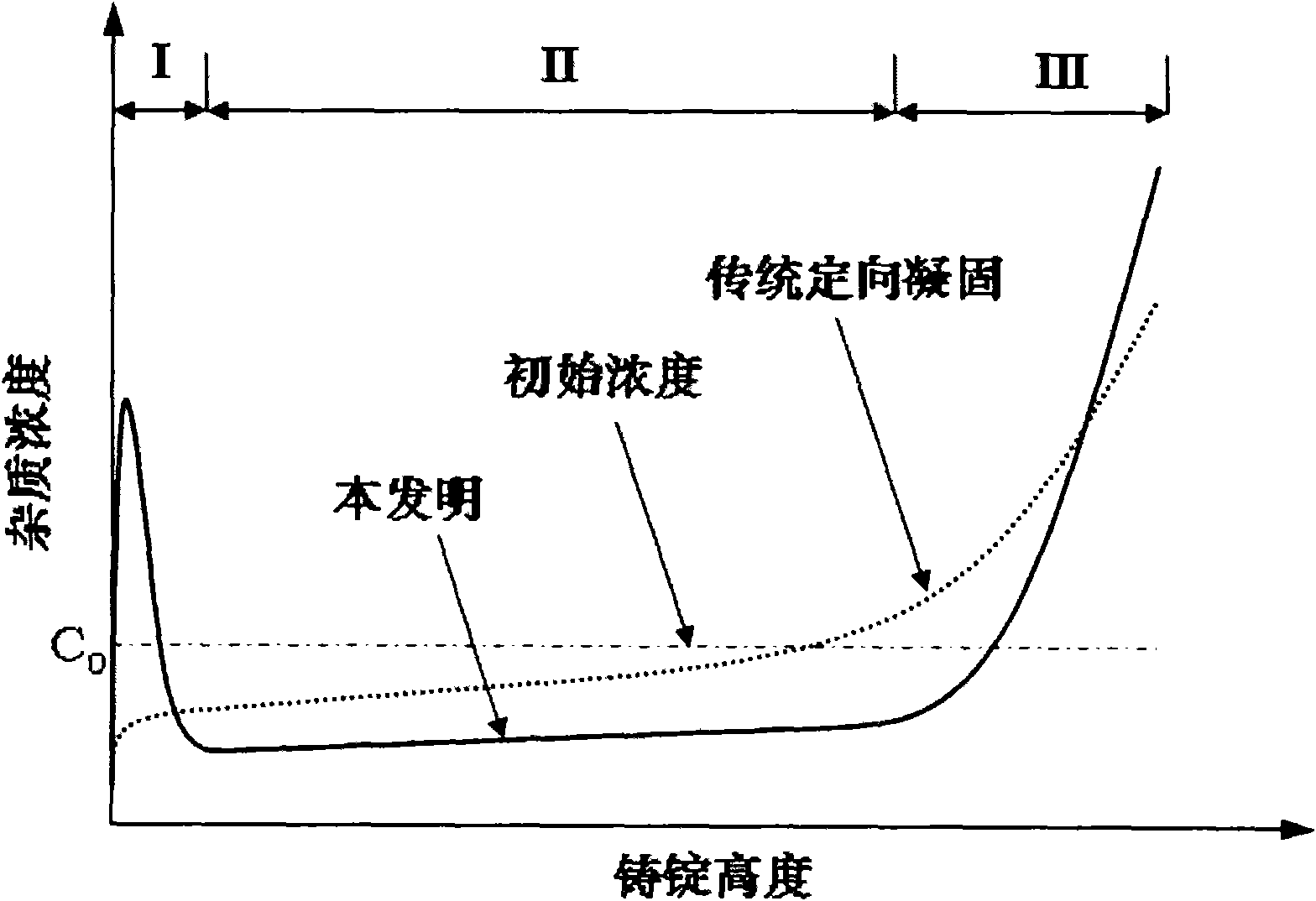
However, some elements, such as boron (B), phosphorus (P), etc., have an equilibrium segregation coefficient in silicon close to 1, and the usual directional solidification process has almost no purification effect on these impurities, so directional solidification requires raw materials to have a lower B , P content, which greatly increases the difficulty of the previous process
Method used
View moreImage
Smart ImageViewing Examples

Examples
Embodiment Construction
Login to View More PUM
 Abstract
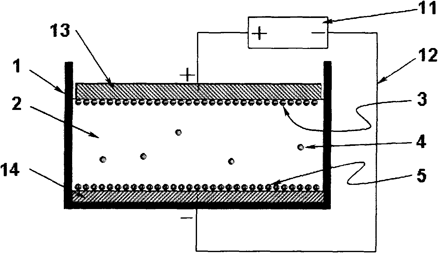
The invention discloses a method for directionally solidifying and purifying polycrystalline silicon under the action of a DC electric field. In the method, the DC electric field which is parallel to the crystal growth direction is applied to fused silicon solution in the growth process of the polycrystalline silicon directional solidification crystal, so that the impurities rapidly move to the electrode direction under the action of the electric field, namely the cation impurities move to the cathode direction, and the anion impurities move to the anode direction. Therefore, the impurity concentration in the crystal growth terminal liquid phase is effectively reduced and the crystal impurity content of subsequent growth is lowered, and polycrystalline silicon ingots of which the directional solidification purity is higher than that of the traditional method for directionally solidifying and purifying the polycrystalline silicon are obtained.
Description
Method for directional solidification and purification of polycrystalline silicon under direct current electric field Technical field The invention relates to the purification of polycrystalline silicon, in particular to a method for purifying polycrystalline silicon by directional solidification under the action of a direct current electric field. Background technique As the main raw material of crystalline silicon solar cells, polysilicon is in increasing demand with the rapid development of the photovoltaic industry. The main source of traditional solar-grade polycrystalline silicon is the remaining pot bottom material when producing electronic grade monocrystalline silicon, and waste materials such as monocrystalline silicon ingot cutting chips. At present, the (improved) Siemens method is the main method for producing high-purity polysilicon. Although the polysilicon obtained by this method has high purity, it has many shortcomings such as high energy consumption, high pr...
Claims
Login to View More Application Information
Patent Timeline
 Patent Type & AuthorityApplications(China)
IPC IPC(8): C30B29/06C30B28/06
Inventor蒋君祥胡建锋熊斌徐璟玉戴宁褚君浩
Owner上海太阳能电池研究与发展中心