

Chip package structure and packaging method thereof
A chip packaging structure and chip packaging technology, applied in the manufacture of electrical components, electrical solid devices, semiconductor/solid devices, etc.
- Summary
- Abstract
- Description
- Claims
- Application Information
AI Technical Summary
Problems solved by technology
Method used
Image

Examples
Embodiment Construction
[0042] Preferred embodiments of the present invention will be described in detail below with reference to the accompanying drawings, but the present invention is not limited to these embodiments. The present invention covers any alternatives, modifications, equivalent methods and schemes made on the spirit and scope of the present invention. In order to provide the public with a thorough understanding of the present invention, specific details are set forth in the following preferred embodiments of the present invention, but those skilled in the art can fully understand the present invention without the description of these details.
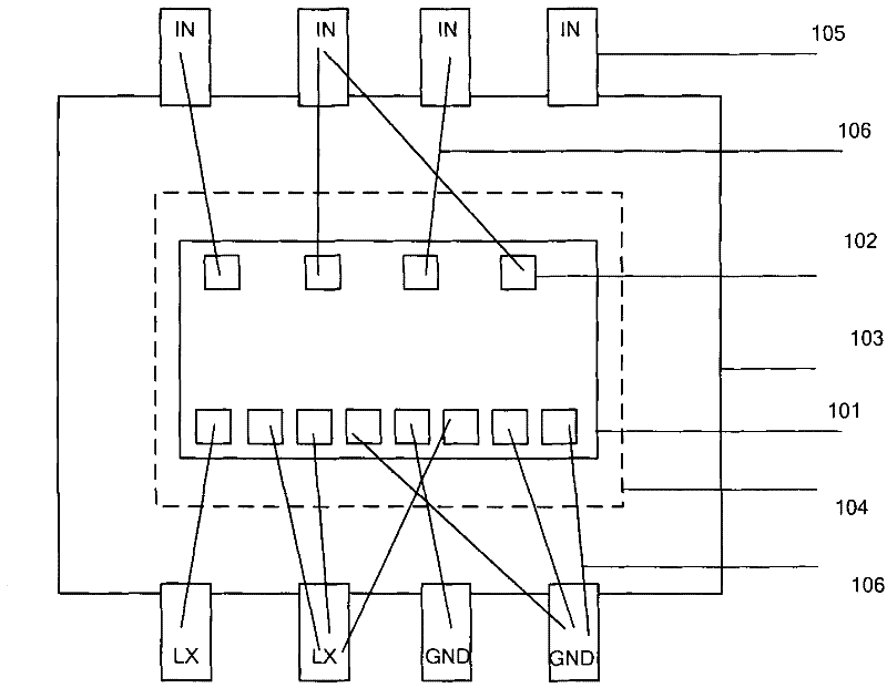
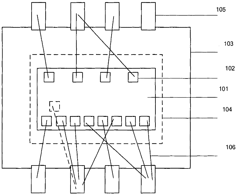
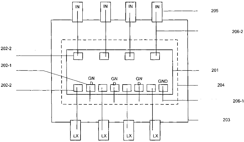
[0043] figure 2 What is shown is a schematic diagram of a chip package structure according to an embodiment of the present invention. The chip package structure of this embodiment includes a chip 201 , a lead frame 203 , a first bonding wire 206 - 1 and a second bonding wire 206 - 2 . The chip 201 has a first contact pad 202-1 and a second cont...
PUM
 Abstract
Description
Claims
Application Information