Schottky junction single-sided electrode crystalline silicon solar cell and preparation method thereof

A solar cell and Schottky junction technology, applied in circuits, photovoltaic power generation, electrical components, etc., can solve the problems of reducing the light-receiving area of ​​solar cells, reducing conversion efficiency, etc., achieving good light trapping effect, improving conversion efficiency, and increasing effective effect of length

Inactive Publication Date: 2010-08-25
江苏华创光电科技有限公司
View PDF3 Cites 10 Cited by
  • Summary
  • Abstract
  • Description
  • Claims
  • Application Information

AI Technical Summary

Problems solved by technology

For the mainstream crystalline silicon solar cells, since the front surface electrodes account for 20% of the surface area, the light-receiving area of ​​the solar cell is reduced, thereby reducing its conversion efficiency

Method used


Image

  • Schottky junction single-sided electrode crystalline silicon solar cell and preparation method thereof
  • Schottky junction single-sided electrode crystalline silicon solar cell and preparation method thereof
  • Schottky junction single-sided electrode crystalline silicon solar cell and preparation method thereof

Examples


Embodiment 1

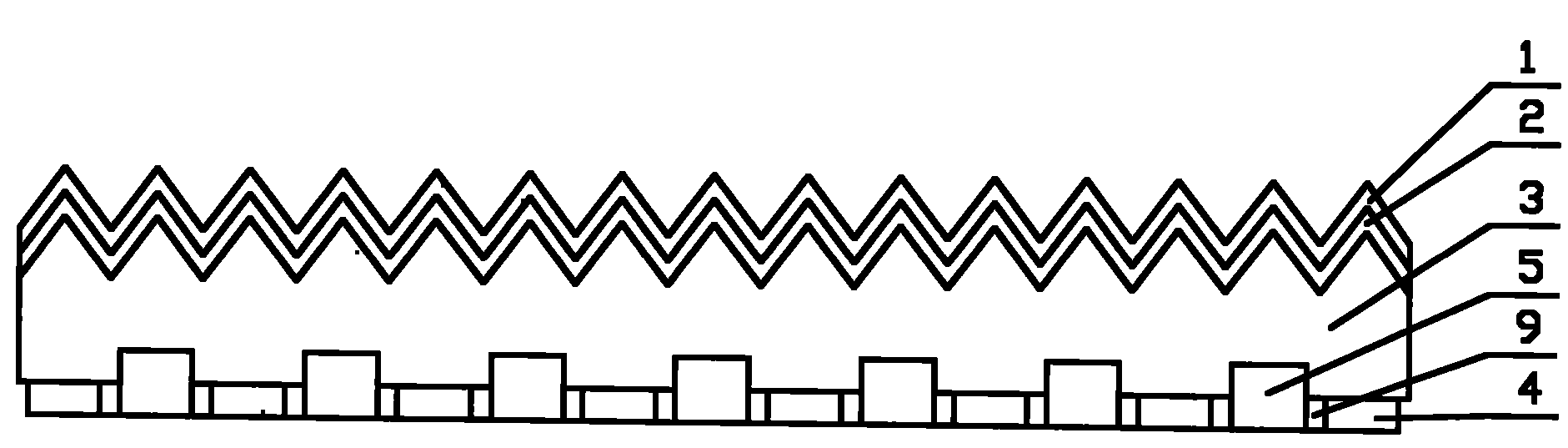
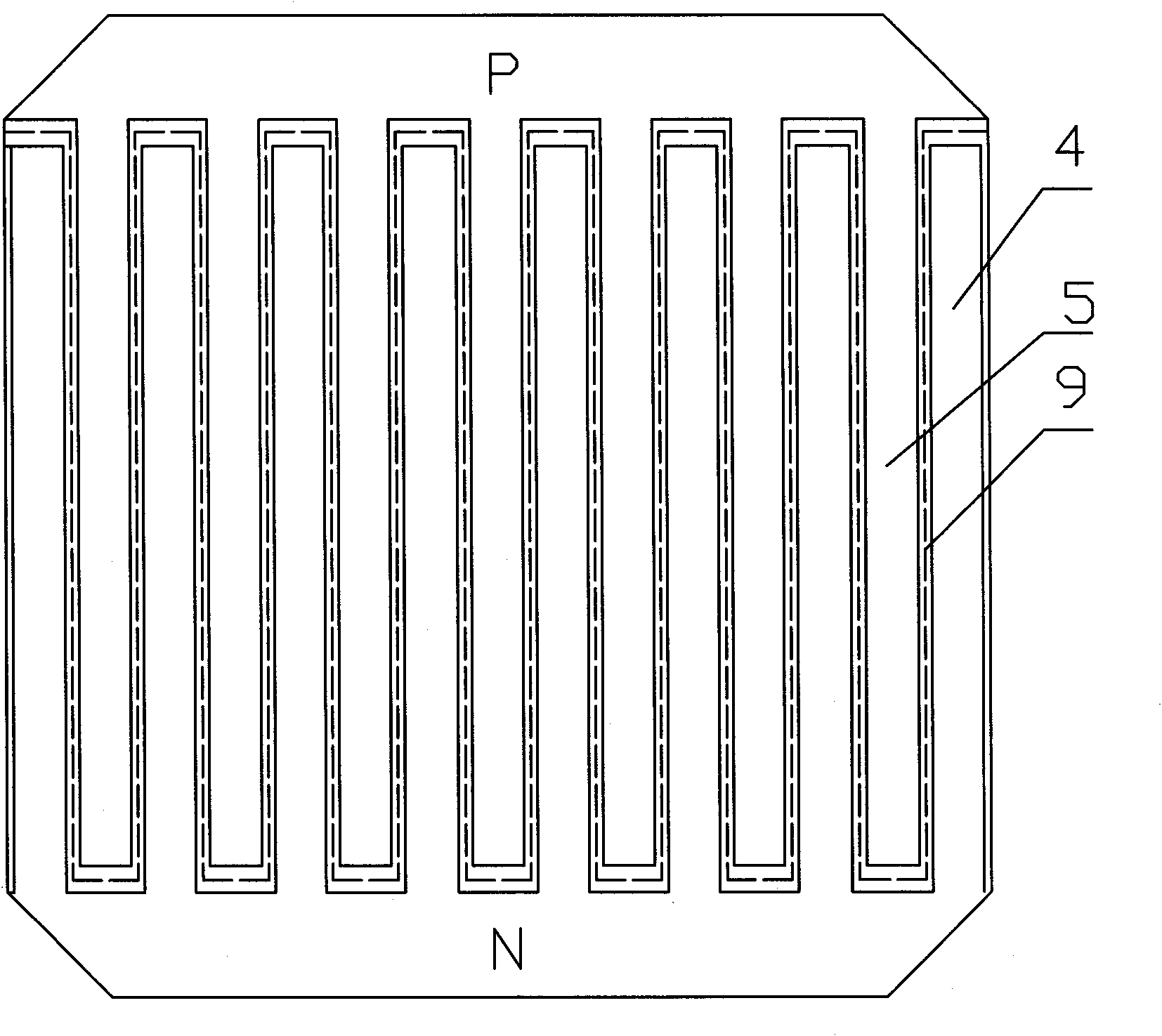
[0054] As shown in Figures 1 and 2, the selected crystal plane is 100 (the crystal plane of silicon is divided into 100, 110, and 111 according to the type, and each crystal plane has different physical and chemical properties), and the size is 156×156×180 μm The N-type substrate 3 has a textured structure on the light-receiving surface of the substrate, and a passivation layer 2 and an anti-reflection layer 1 are provided. Then set the grid-shaped aluminum negative electrode 5 on the backlight surface, the aluminum negative electrode 5 forms a Schottky grid junction with a certain depth with the crystalline silicon, and then set the grid-shaped silver-aluminum lead-out positive electrode 4 forming ohmic contact with the backlight surface at the remaining positions , There is a certain gap 9 between the positive electrode 4 and the aluminum negative electrode 5 .

Embodiment 2

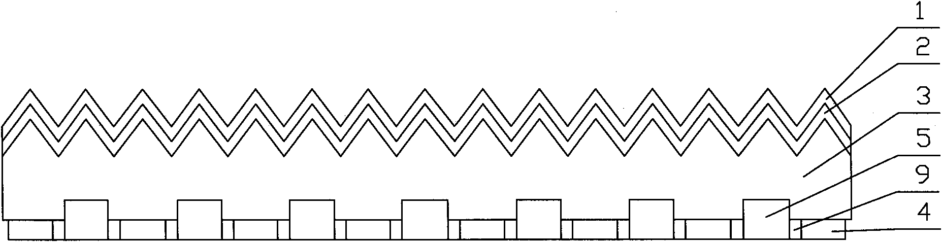
[0056] As shown in Figures 3 and 4, select an N-type substrate 3 with a crystal plane of 100 and a size of 156×156×100 μm, make a textured structure on the light-receiving surface of the substrate, and set a passivation layer 2 and an anti-reflection layer 1. An N+ doped layer 8 is arranged on the backlight surface of the substrate, and then a grid-shaped aluminum layer 6 with a Schottky PN junction penetrating the N+ doped layer is arranged on the N+ doped layer, and then a grid-shaped silver-aluminum lead-out positive electrode is arranged on the remaining positions. There is a certain gap 9 between the electrode 7 , the positive electrode 7 and the grid-shaped aluminum layer 6 .

Embodiment 3

[0058] 1) Select an N-type substrate with a crystal plane of 100 and a size of 156×156×100 μm, and send it to a texturing equipment for routine cleaning and texturing to produce a textured surface with a refractive index of 2.2. 2) Plating a passivation layer and an anti-reflection layer on the suede surface of the light-receiving surface. 3) Screen-print grid-shaped aluminum paste on the backlight surface of the substrate with a grid width of 0.3 mm. 4) Selectively irradiate the position of the aluminum paste on the substrate with a continuous strong laser, so that the temperature of the substrate rises to 1400°C instantaneously, and continue to irradiate for 25 minutes. 5) Print grid-shaped silver-aluminum electrodes on other positions on the backlight surface. 6) Perform aluminum back field sintering to complete the solar cell preparation.


PUM

PropertyMeasurementUnit
Depthaaaaaaaaaa
Thicknessaaaaaaaaaa
Sizeaaaaaaaaaa

Abstract

The invention discloses a Schottky junction single-sided electrode crystalline silicon solar cell. In the cell, the backlight face of an N-type substrate is provided with a negative electrode which forms a Schottky junction together with the N-type substrate and a positive electrode which is matched with the negative electrode in shape, wherein the positive electrode and the N-type substrate are in ohmic contact; and a clearance is reserved between the negative electrode and the positive electrode. The invention also discloses a preparation method, which comprises: texturing the N-type substrate, and plating a light receiving surface with a passive layer and a reflective layer; forming the aluminum negative electrode on the backlight face of the N-type substrate by screen printing, wherein the aluminum negative electrode is shaped like a grid or comb; irradiating the aluminum negative electrode with strong laser to allow aluminum to permeate into a chip to form the Schottky junction; forming the metal positive electrode on the backlight face of the N-type substrate, which is crossed with the aluminum negative electrode and has the same shape as the aluminum negative electrode, by screen printing to form the positive electrode of the cell; and sintering the substrate to make the metal positive electrode in ohmic contact with the backlight face of the N-type substrate. The front face of the cell is not blocked and therefore can receive 10 to 20 percent of sunlight.

Description

technical field [0001] The invention relates to the field of crystalline silicon solar cells, in particular to a Schottky junction single-sided electrode crystalline silicon solar cell and a preparation method thereof. Background technique [0002] Solar energy, as a clean energy without any pollution, and the possibility of solar power as one of the main sources of power supply, have increasingly attracted people's attention. The key to solving this technology lies in the reduction of solar cell production costs and the improvement of conversion efficiency. For the mainstream crystalline silicon solar cells, since the front surface electrodes account for 20% of the surface area, the light-receiving area of ​​the solar cell is reduced, thereby reducing its conversion efficiency. [0003] Relevant technicians in the photovoltaic industry have made a lot of technological innovations and improvements on the basis of the traditional structure in order to improve the conversion ...

Claims


Application Information

Patent Timeline
IPC IPC(8): H01L31/042H01L31/07H01L31/0352H01L31/0224H01L31/18
CPCY02E10/50Y02P70/50
Inventor 张宏勇刘莹
Owner 江苏华创光电科技有限公司
Why Eureka
Try Eureka