

Production method of groove-type power semiconductor with low grid charge and structure thereof
A technology for power semiconductors and manufacturing methods, applied in semiconductor/solid-state device manufacturing, semiconductor devices, circuits, etc., can solve problems such as limited bottom area, and achieve the effect of reducing switching loss, reducing overlapping area, and improving switching speed
- Summary
- Abstract
- Description
- Claims
- Application Information
AI Technical Summary
Problems solved by technology
Method used
Image

Examples
no. 1 example
[0040] The invention provides a method for manufacturing a low gate charge trench power semiconductor and its structure. The method utilizes a polysilicon spacer to reduce the overlapping area (overlap) between the polysilicon and the bottom of the trench, and cooperates with a low The role of the metal silicide with high resistivity to achieve the effect of reducing the gate-drain capacitance (Cgd) and reducing the resistance, thereby reducing the switching loss. see Figure 1A to Figure 1M , which is the first embodiment of the manufacturing method of the present invention, comprising the following steps:
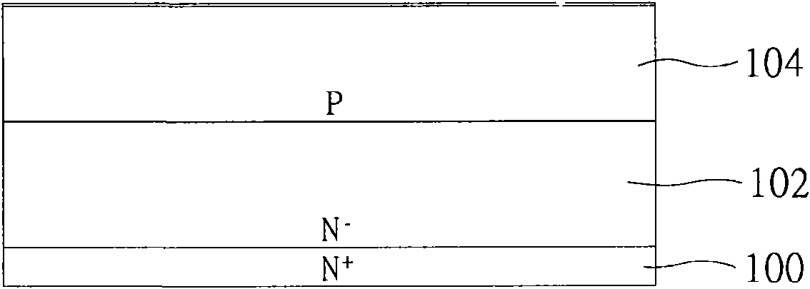
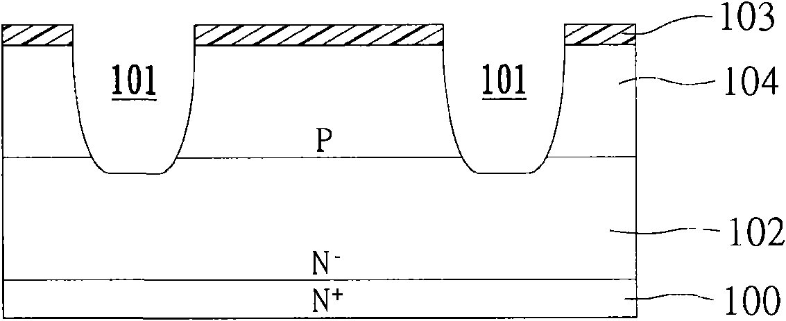
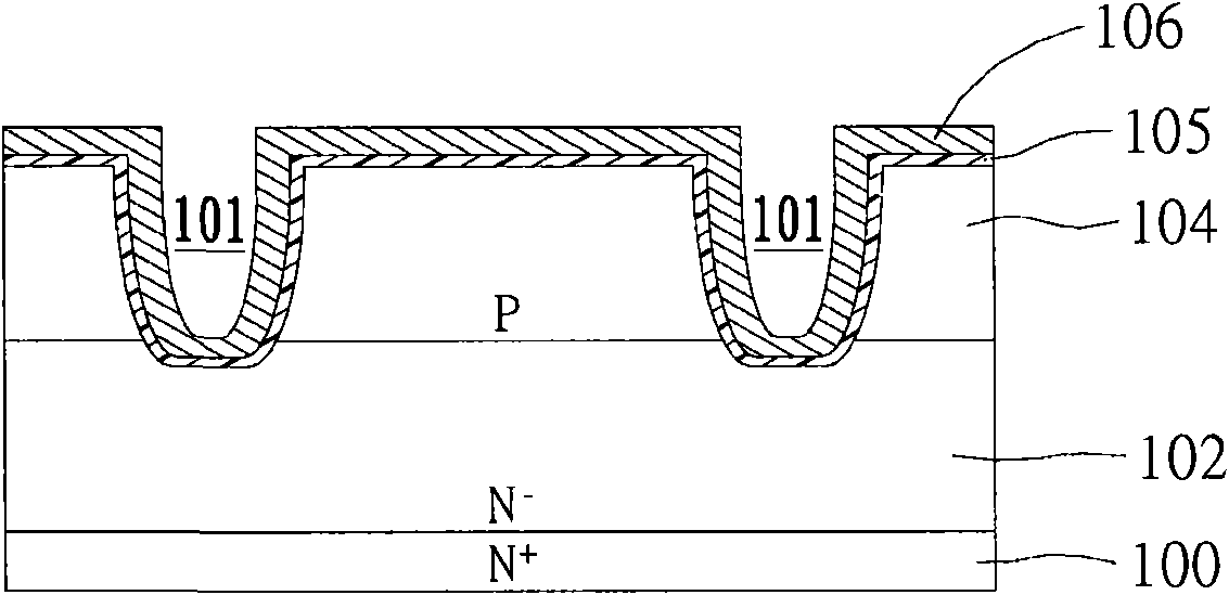
[0041] First, if Figure 1A As shown, a first conductive type semiconductor substrate 100 is provided, and a first conductive type epitaxial layer 102 is formed on the first conductive type semiconductor substrate 100, and a second conductive type body region 104 is implanted and Diffusion process is formed on the upper portion of the first conductivity type epitaxial la...
no. 2 example
[0055] Please refer to Figure 2A to Figure 2I , which is a second embodiment of the present invention, which includes the following steps:
[0056] Figure 2A to Figure 2D The steps are the same as those in the first embodiment, so the following will focus on Figure 1A to Figure 1D Make a simple explanation.
[0057] First, if Figure 2A As shown, a first conductive type semiconductor substrate 200 is provided, and a first conductive type epitaxial layer 202 is formed on the first conductive type semiconductor substrate 200, and a second conductive type body region 204 is formed by ion implantation It is formed on the upper part of the epitaxial layer 202 of the first conductivity type by a diffusion process, and the related ion doping concentration can refer to the above description.
[0058] Subsequently, if Figure 2B As shown, a plurality of trenches 201 are formed in the epitaxial layer 202 of the first conductivity type, and each trench 201 penetrates the body reg...
PUM
 Abstract
Description
Claims
Application Information