Inverse piezoelectric nano semiconductor generator

A nano-semiconductor, semiconductor technology, applied in the direction of generator/motor, piezoelectric effect/electrostrictive or magnetostrictive motor, electrical components, etc., can solve the high cost of motor manufacturing and assembly, generator assembly and operation mechanism Harshness, mechanical breakage of nanowires, etc.

Inactive Publication Date: 2010-10-13
LIAONING NORMAL UNIVERSITY
View PDF6 Cites 5 Cited by
  • Summary
  • Abstract
  • Description
  • Claims
  • Application Information

AI Technical Summary

Problems solved by technology

However, under the action of strong external mechanical vibration force, the nanowires and metal needle tips of this nanogenerator will produce large mechanical deformation, which is prone to mechanical breakage of the nanowires and affects its service life. At the same time, the upper and lower nanometer The assembly mode that requires precise contact between the lines also makes the assembly and operation mechanism of this generator more demanding;
[0007] 3. In order to collect the piezoelectric polarization charge generated by the mechanical deformation of the semiconductor and form the unidirectional conduction effect of the current, the upper polarization charge collection unit of this nanogenerator needs to be plated with a layer of work function greater than that of the N-type ZnO semiconductor material. Functional Au or Pt and other precious metal materials, the motor manufacturing and assembly costs are relatively high;
[0008] 4. The output power and current intensity that the unit area device of this kind of nano generator can provide is still small, so that the scope of application of this kind of nano generator is limited to a certain extent

Method used


Image

  • Inverse piezoelectric nano semiconductor generator
  • Inverse piezoelectric nano semiconductor generator
  • Inverse piezoelectric nano semiconductor generator

Examples


Embodiment Construction

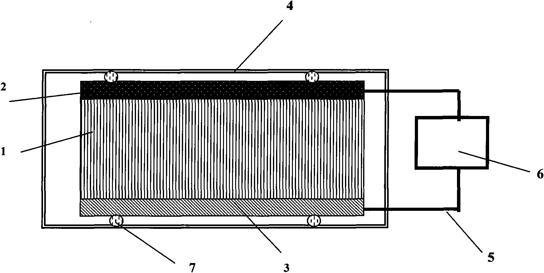
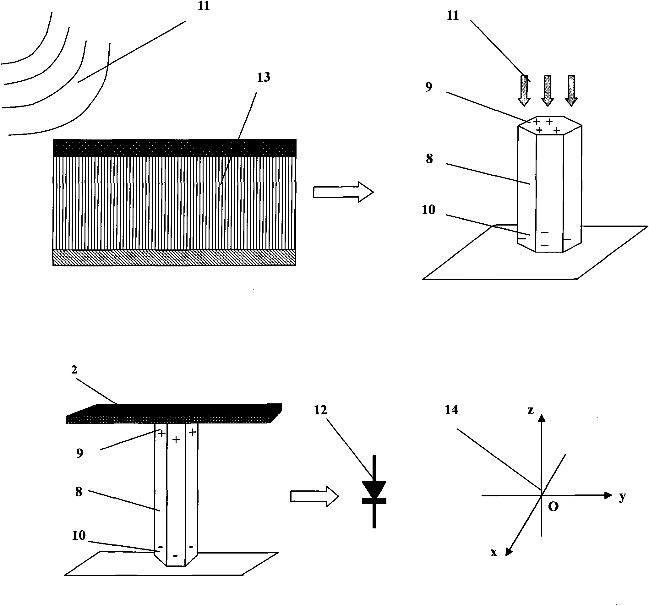
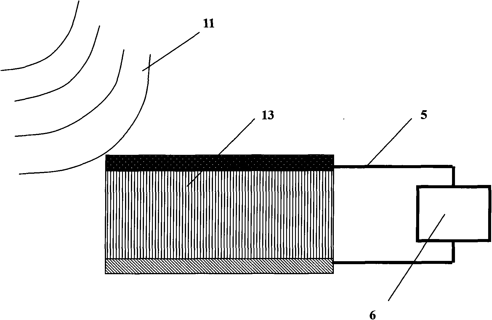
[0029] The present invention will be further described below in conjunction with the accompanying drawings. Such as figure 1 As shown, a reverse piezoelectric nano-semiconductor generator includes a semiconductor nanowire array 1, a metal sheet 2, a housing 4 and an external circuit 5, and the semiconductor nanowire array 1 is composed of an oriented semiconductor with reverse piezoelectric and polarization characteristics composed of nanowires, grown on the corresponding conductive metal substrate 3, the metal sheet 2 is in close contact with the upper end of the semiconductor nanowire array 1 placed upward, and the semiconductor nanowire array 1 and the metal sheet 2 pass through the upper and lower After lamination and contact, it is directly fixed in the shell 4 by the suspension spring system 7, and is connected to the external circuit 5; the semiconductor nanowire array 1 is a semiconductor ZnO that is directly grown on a metal Zn substrate by a hydrothermal synthesis p...


PUM


Abstract

The invention discloses an inverse piezoelectric nano semiconductor generator, which comprises a semiconductor nano-wire array, a metal sheet, a shell and an external circuit. The nano-wire array consists of oriented semiconductor nano-wires with inverse piezoelectricity and polarization characteristics and is grown on a corresponding conductive metal substrate; the metal sheet is tightly contacted with the other side of the semiconductor nano-wire array; and the semiconductor nano-wire array and the metal sheet are directly fixed in the shell through a suspension spring system after up-and-down laminated contact and connected with the external circuit. When spatial electromagnetic radiation signals are acted on the nano-wires, the nano-wires generate inverse piezoelectricity and polarization phenomenon, and positive and negative charges are accumulated on the surfaces of the nano-wires. Meanwhile, Schottky contact effect causing unidirectional conduction of current is formed between the contact faces of a metal and an N-type semiconductor, and polarization charges on the surfaces of the nano-wires are directly output to the external circuit in a form of electronic current so as to finish energy conversion from electromagnetic radiation energy to electrical energy.

Description

technical field [0001] The invention relates to the technical fields of nanometer power generation, microelectromechanical machinery and power supply, and relates to an inverse piezoelectric nanometer semiconductor generator for converting electromagnetic radiation energy in space into electric energy. Background technique [0002] With the advent of the information age, people have more and more opportunities to use and contact various electronic instruments and electronic products in their work and daily life. Various household appliances, electronic equipment, office automation equipment, mobile communication equipment and other electrical devices only When they are in working use, they will radiate electromagnetic waves to their surroundings. If the human body is exposed to electromagnetic radiation doses exceeding the safe range for a long time, the cells will be killed or killed in a large area, which will have a very adverse effect on human health. . [0003] Space r...

Claims


Application Information

Patent Timeline
Patent Type & Authority Applications(China)
IPC IPC(8): H02N2/18
Inventor 李梦轲张竞王军艳冯秋菊耿渊博姜春华
Owner LIAONING NORMAL UNIVERSITY
Why Eureka
Try Eureka