Double-input operational amplifier shared margin gain amplifying circuit

A gain amplifier circuit, operational amplifier technology, applied in the direction of amplification control, differential amplifier, DC-coupled DC amplifier, etc., can solve problems such as reducing the accuracy of analog-to-digital converters, eliminate memory effects, eliminate clock feedthrough, improve The effect of precision

Inactive Publication Date: 2010-10-13
FUDAN UNIV
View PDF3 Cites 21 Cited by
  • Summary
  • Abstract
  • Description
  • Claims
  • Application Information

AI Technical Summary

Problems solved by technology

Memory effects are signal dependent and degrade the accuracy of the ADC

Method used


Image

  • Double-input operational amplifier shared margin gain amplifying circuit
  • Double-input operational amplifier shared margin gain amplifying circuit
  • Double-input operational amplifier shared margin gain amplifying circuit

Examples


Embodiment Construction

[0031] The present invention will be described in further detail below in conjunction with the accompanying drawings and specific embodiments.

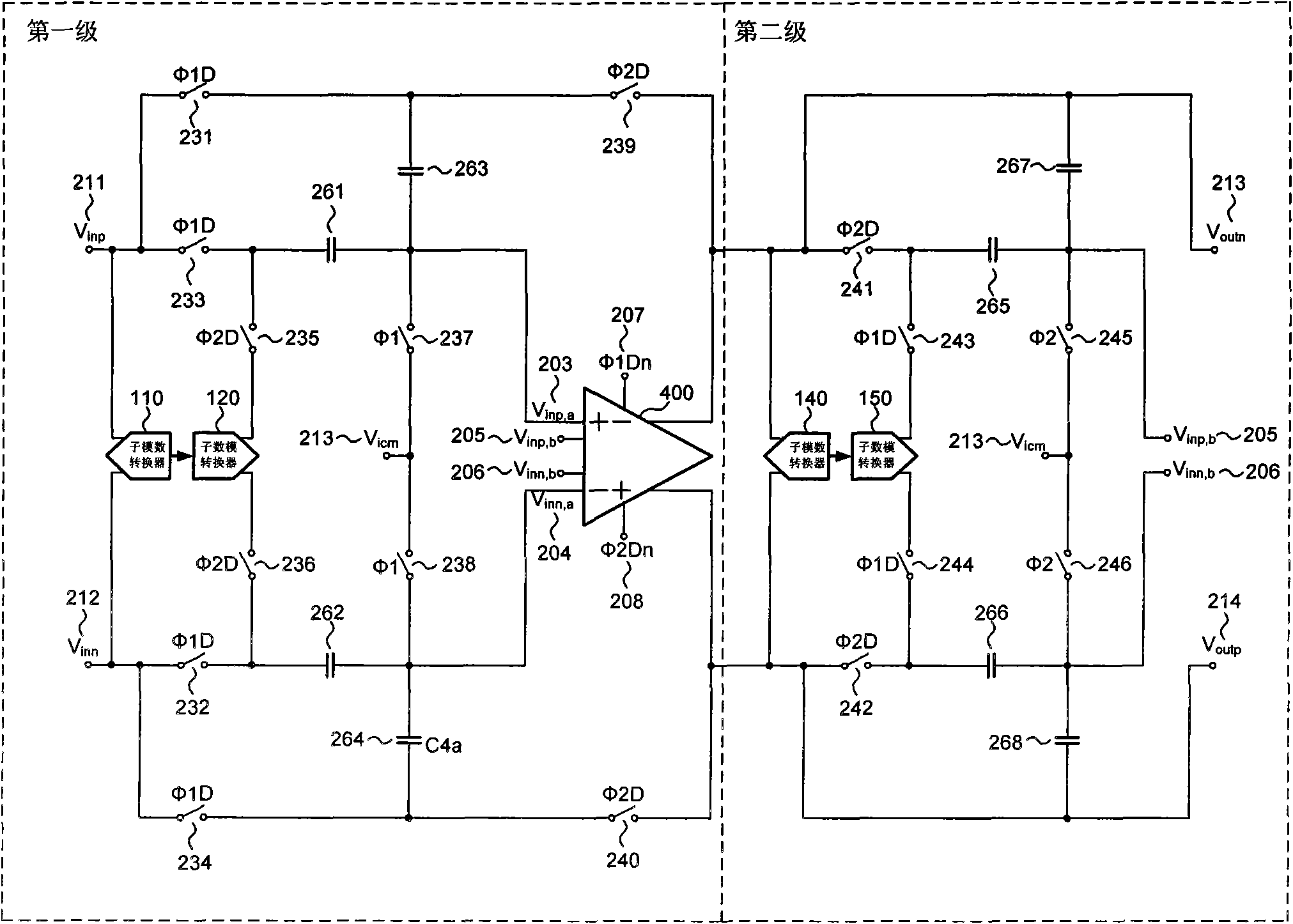
[0032] figure 2Structural schematic diagram of the residual gain amplification circuit shared by the dual-input operational amplifier used in the present invention, including a built-in double differential input pair operational amplifier circuit 400, a sub-analog-to-digital conversion circuit 110, a sub-analog-to-digital conversion circuit 140, and a sub-digital-to-analog hybrid Circuit 120, sub-digital-analog hybrid circuit 140, sampling and feedback capacitors 261, 262, 263, 264, 265, 266, 267, 268, switches 231, 232, 233, 234, 235, 236, 237, 238, 239, 240 , 241, 242, 234, 244, 245, 246, common mode input voltage 215.

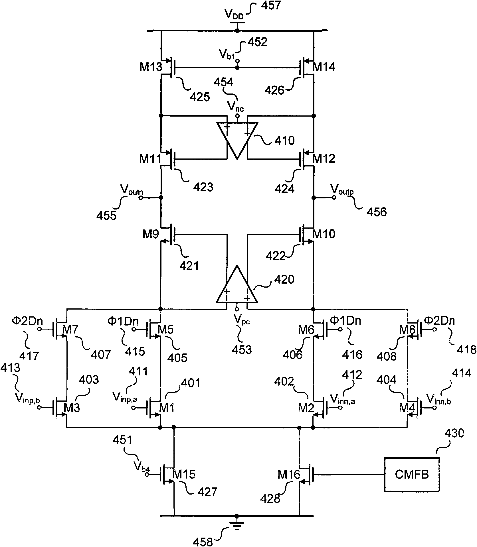
[0033] image 3 A schematic diagram of a dual differential input pair operational amplifier circuit 400 built into a switch used in the present invention, including two pairs of operational amplifier differential...


PUM


Abstract

The invention belongs to the technical field of data converters in integrated circuit design, and discloses a double-input operational amplifier shared margin gain amplifying circuit. The amplifying circuit comprises a double-input operational amplifier, a clock generating circuit, a sub digital-to-analog converter, a sub analog-to-digital converter, a capacitor, a switch and the like. Two groups of differential input pair tubes are controlled through the switch controlled by bidirectional overlapped clocks and embedded inside the operational amplifier by adopting the operational amplifier of two groups of input differential pairs and are alternately used at two phases of the clocks, and meanwhile the input differential pairs are alternately reset to a common-mode input voltage so as to fully eliminate the influence of memory effect and inter-stage feed-through in the traditional circuit, improve the signal establishing precision under the condition of keeping the same area, power consumption and circuit complexity and further improve the precision of analog-to-digital conversion.

Description

technical field [0001] The invention belongs to the technical field of data converters in integrated circuit design, and in particular relates to a margin gain amplifying circuit shared by dual-input operational amplifiers. Background technique [0002] The analog-to-digital converter is an important module in the communication circuit, which realizes the conversion from analog signal to digital signal. For mobile handheld terminals with more and more functions, due to the limitation of weight and volume, energy can only be provided by a limited battery, so there is an urgent need for low power consumption technology of electronic devices. The advantage in low-power technology means that it will occupy a larger share and obtain higher profits in this fast-growing market. [0003] In addition, the increase in power consumption will cause the chip to heat up, thereby reducing the reliability and service life of the circuit. The temperature rise of the chip will cause a serie...

Claims


Application Information

Patent Timeline
Patent Type & Authority Applications(China)
IPC IPC(8): H03G3/20H03F3/45
Inventor 尹睿唐长文
Owner FUDAN UNIV
Why Eureka
Try Eureka