Ferroelectric metal hetero-junction based memristor and preparation method thereof

A technology of memristor and electric lithium niobate, which is applied in the field of microelectronic materials, can solve the problems of few reports and difficult to predict the application prospect of memristor

Inactive Publication Date: 2010-10-20
NANJING UNIV
View PDF4 Cites 24 Cited by
  • Summary
  • Abstract
  • Description
  • Claims
  • Application Information

AI Technical Summary

Problems solved by technology

[0004] Because of its special electrical properties, memristors can bring unpredictable broad application prospects, especially the use of memristor circuits, it is possible to simulate the working mode of brain synapses, and provide the possibility for the realization of artificial neural networks
However, the memristor behavior of other materials and structures has been rarely reported except for the HP lab findings.

Method used


Image

  • Ferroelectric metal hetero-junction based memristor and preparation method thereof
  • Ferroelectric metal hetero-junction based memristor and preparation method thereof
  • Ferroelectric metal hetero-junction based memristor and preparation method thereof

Examples


Embodiment 1

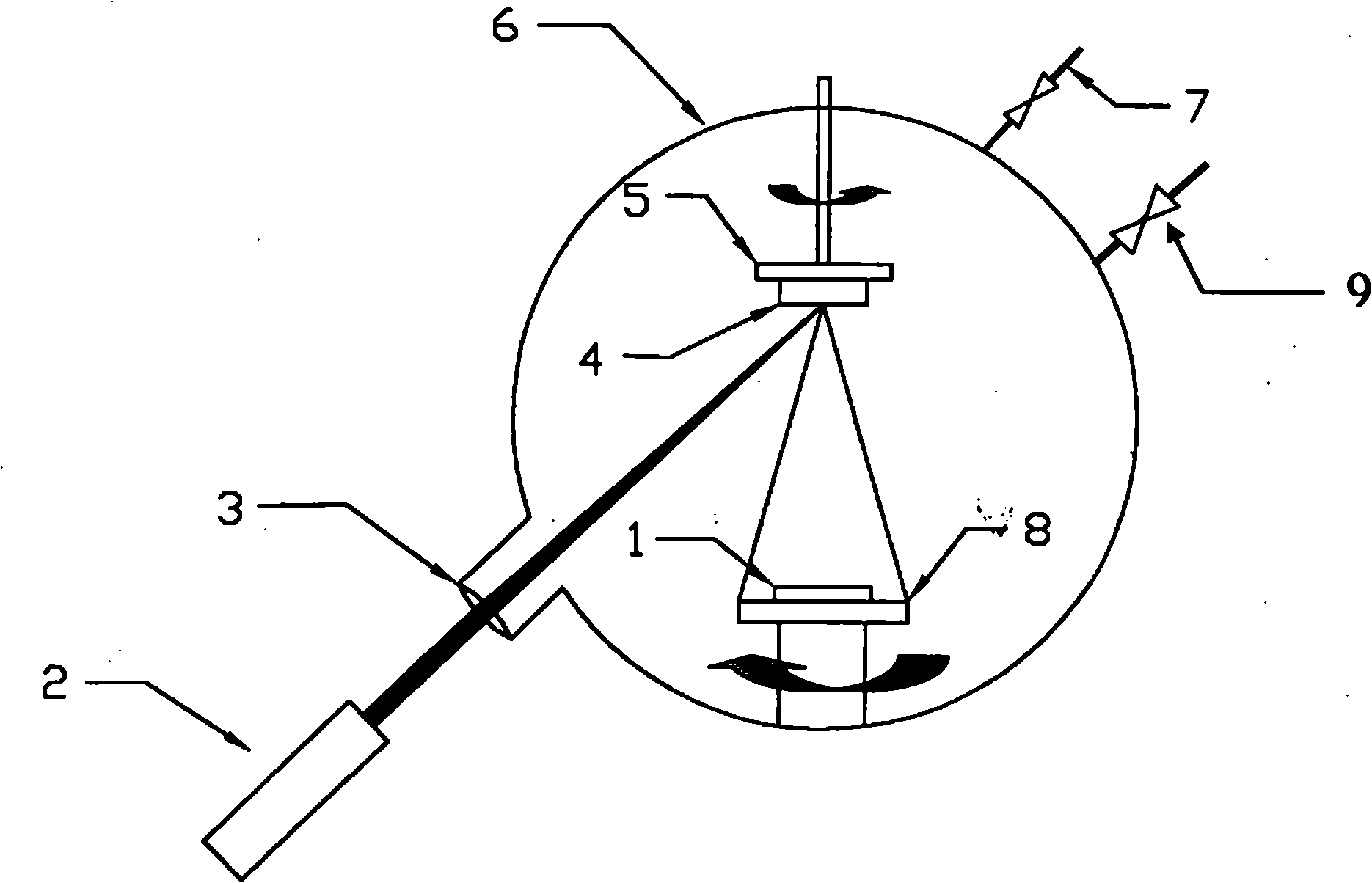
[0036] Embodiment 1: the preparation method of ferroelectric lithium niobate, its preparation steps are as follows:

[0037] a) fixing the single crystal LN target material 4 on the target table 5 of the pulsed laser deposition film-making system, fixing the substrate 1 on the substrate table 8, and placing them in the growth chamber 6 of the pulsed laser deposition film-making system;

[0038] b) Use a vacuum pump to evacuate the growth chamber 6 to 0.8×10 through the interface valve 7 of the mechanical pump and the molecular pump -4 Below Pa, turn off the molecular pump;

[0039] c) Adjust the intake valve 9 so that the pressure of the flowing oxygen in the growth chamber is 25-35 Pa;

[0040] d) using a resistance heating furnace to heat the substrate table 5 to raise the temperature of the substrate 4 to 600-650°C;

[0041] e) rotating the substrate table 5 and the target table 8;

[0042] f) Start the KrF excimer laser 2 with a wavelength of 248nm, a pulse width of 30n...

Embodiment 2

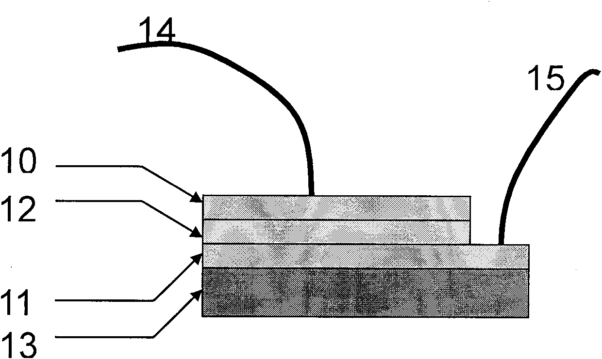
[0045] Embodiment 2. The preparation method of the sandwich structure memristor unit based on the ferroelectric metal junction, the specific preparation steps are as follows:

[0046] a) on Pt / Ti / SiO 2 / Si(111) substrate, grow a LN film with a thickness of about 50nm to 100nm by PLD method, and press a corner of the substrate with a clamp during the deposition process, so that the leaked part of the Pt film will be used as the lower electrode;

[0047] b) Take out the crystallized LN thin film from the PLD growth chamber, cover it with a mask, and use magnetron sputtering or other coating methods to grow the Pt electrode with a thickness of 100nm-150nm, thus forming a miniature sandwich structure; if Au / Ti / SiO 2 / Si(111) substrate, the growth of the upper electrode Au obtained basically the same results;

[0048] c) Finally, the copper leads 14, 15 are respectively connected from the upper and lower electrode films 10, 11, thus forming a memristor unit.


PUM

PropertyMeasurementUnit
thicknessaaaaaaaaaa

Abstract

The invention relates to a ferroelectric metal hetero-junction based memristor; wherein the memristor material-ferroelectric lithium niobate is prepared by a pulse laser deposition system; monocrystal LN target material (4) is fixed on a target platform (5) of the pulse laser deposition system, and is placed in a growth chamber (6) of a pulse laser deposition film-making system; the vacuum in the growth chamber is pumped to be below 0.8*10-4Pa, oxygen gas flows in, and the oxygen pressure is from 25 to 35Pa, the substrate temperature is heated from 600-650 DEG; a KrF excimer laser is started, and the deposition time is determined according to monopulse energy; in-situ 500-650 DEG annealing is carried out 20-90min; the film has spontaneous polarization and 180-degree domain boundary; the memristor ferroelectric lithium niobate film is clamped between two metal electrode films to form a memristor unit with a miniature sandwich structure; the device can be applied to a high-density low-energy-consumption nonvolatile resistance random access memory.

Description

1. Technical field [0001] The invention belongs to the field of microelectronic materials, in particular to a ferroelectric material lithium niobate (LiNbO 3 , referred to as LN) and a memristor element based on a ferroelectric metal heterojunction structure. 2. Background technology [0002] In 1971, Professor Leon Chua of the University of California, Berkeley predicted theoretically that there should be a fourth circuit component other than resistors, capacitors, and inductors. Features and functions. The main feature of the memristor is that it can change the resistance state with the change of the applied electric quantity, thereby realizing the memory function. Such electronic components could open up the possibility of faster and more energy-efficient instant-on PCs, as well as analog computers and artificial neural networks that process information like the human brain. [0003] Thirty-seven years after the theoretical model of the memristor was proposed, Strukov ...

Claims


Application Information

Patent Timeline
Patent Type & Authority Applications(China)
IPC IPC(8): C30B23/02C30B29/30C30B33/02H01L45/00
Inventor 李海涛夏奕东徐波国洪轩殷江刘治国
Owner NANJING UNIV
Why Eureka
Try Eureka